Applications information – Rainbow Electronics ADC0848 User Manual
Page 10
Applications Information
(Continued)
‘‘a’’ input and then the ‘‘b’’ inputs is
of a clock period
The change in the common-mode voltage during this short
time interval can cause conversion errors For a sinusoidal
common-mode signal this error is
V
ERROR(MAX)
e
V
peak
(2
q
f
CM
)
c
0 5
c
t
C
8
J
where f
CM
is the frequency of the common-mode signal
V
peak
is its peak voltage value and t
C
is the conversion time
For a 60 Hz common-mode signal to generate a
LSB
error (
5 mV) with the converter running at 40 mS its peak
value would have to be 5 43V This large a common-mode
signal is much greater than that generally found in a well
designed data acquisition system
3 2 Input Current
Due to the sampling nature of the analog inputs short dura-
tion spikes of current enter the ‘‘a’’ input and exit the ‘‘b’’
input at the clock edges during the actual conversion These
currents decay rapidly and do not cause errors as the inter-
nal comparator is strobed at the end of a clock period By-
pass capacitors at the inputs will average these currents
and cause an effective DC current to flow through the out-
put resistance of the analog signal source Bypass capaci-
tors should not be used if the source resistance is greater
than 1 kX
3 3 Input Source Resistance
The limitation of the input source resistance due to the DC
leakage currents of the input multiplexer is important A
worst-case leakage current of
g
1 mA over temperature will
create a 1 mV input error with a 1 kX source resistance An
op amp RC active low pass filter can provide both imped-
ance buffering and noise filtering should a high impedance
signal source be required
4 0 OPTIONAL ADJUSTMENTS
4 1 Zero Error
The zero of the A D does not require adjustment If the
minimum analog input voltage value V
IN(MIN)
is not ground
a zero offset can be done The converter can be made to
output 0000 0000 digital code for this minimum input voltage
by biasing any V
IN
(b) input at this V
IN(MIN)
value This is
useful for either differential or pseudo-differential modes of
input channel configuration
The zero error of the A D converter relates to the location
of the first riser of the transfer function and can be mea-
sured by grounding the V
b
input and applying a small mag-
nitude positive voltage to the V
a
input Zero error is the
difference between actual DC input voltage which is neces-
sary to just cause an output digital code transition from 0000
0000 to 0000 0001 and the ideal
LSB value (
LSBe9 8
mV for V
REF
e
5 000 V
DC
)
4 2 Full-Scale
The full-scale adjustment can be made by applying a differ-
ential input voltage which is 1
LSB down from the desired
analog full-scale voltage range and then adjusting the mag-
nitude of the V
REF
input for a digital output code changing
from 1111 1110 to 1111 1111
4 3 Adjusting for an Arbitrary Analog Input Voltage
Range
If the analog zero voltage of the A D is shifted away from
ground (for example to accommodate an analog input sig-
nal which does not go to ground) this new zero reference
should be properly adjusted first A V
IN
(a) voltage which
equals this desired zero reference plus
LSB (where the
LSB is calculated for the desired analog span 1 LSB e
analog span 256) is applied to selected ‘‘a’’ input and the
zero reference voltage at the corresponding ‘‘b’’ input
should then be adjusted to just obtain the 00
HEX
to 01
HEX
code transition
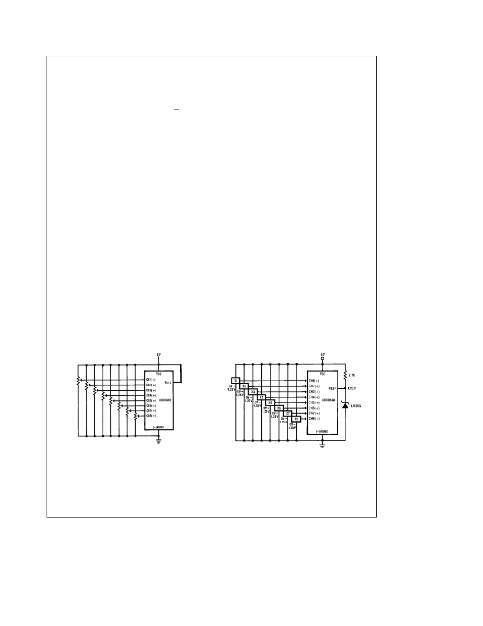
TL H 5016 – 16
a) Ratiometric
TL H 5016 – 17
b) Absolute with a Reduced Span
FIGURE 2 Referencing Examples
10