Rainbow Electronics MAX16832C User Manual
Page 2
MAX16832A/MAX16832C
2MHz, High-Brightness LED Drivers with
Integrated MOSFET and High-Side Current Sense
2
_______________________________________________________________________________________
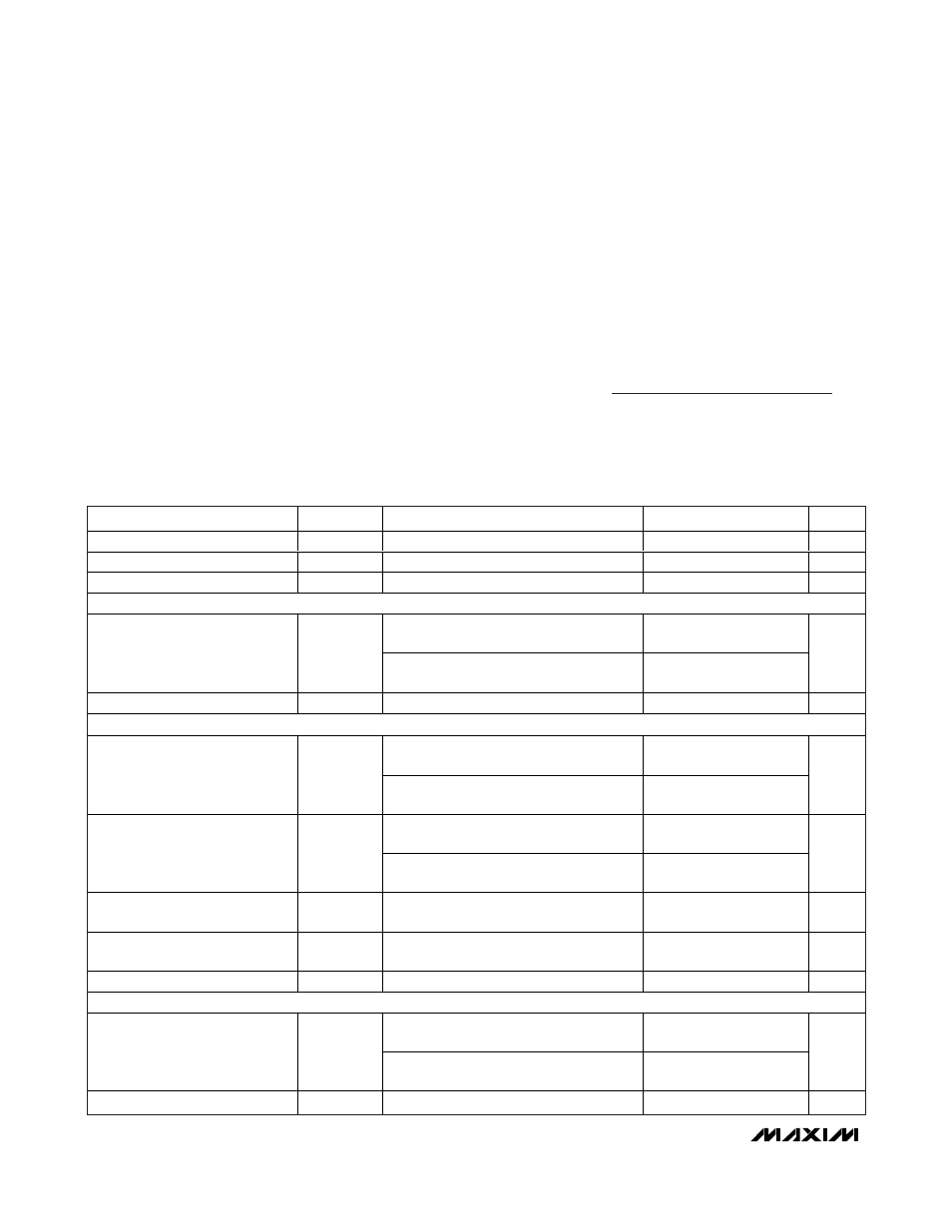
ABSOLUTE MAXIMUM RATINGS
ELECTRICAL CHARACTERISTICS
(V
IN
= +24V, V
DIM
= V
IN
, T
A
= T
J
= -40°C to +125°C, unless otherwise noted. Typical values are at T
A
= +25°C.)
Stresses beyond those listed under “Absolute Maximum Ratings” may cause permanent damage to the device. These are stress ratings only, and functional
operation of the device at these or any other conditions beyond those indicated in the operational sections of the specifications is not implied. Exposure to
absolute maximum rating conditions for extended periods may affect device reliability.
Note 1: Package thermal resistances were obtained using the method described in JEDEC specification JESD51-7, using a four-
layer board. For detailed information on package thermal considerations, refer to
www.maxim-ic.com/thermal-tutorial
.
IN, CS, LX, DIM to GND .........................................-0.3V to +70V
TEMP_I to GND .......................................................-0.3V to +6V
PGND to GND ......................................................-0.3V to +0.3V
CS to IN .................................................................-0.3V to +0.3V
Maximum Current into Any Pin
(except IN, LX, and PGND).............................................20mA
Continuous Power Dissipation (T
A
= +70°C)
8-Pin SO (derate 23.3mW/°C above +70°C)...........1860.5mW
Junction-to-Ambient Thermal Resistance (
θ
JA
) (Note 1) .....43°C/W
Operating Temperature Range .........................-40°C to +125°C
Junction Temperature ......................................................+150°C
Storage Temperature Range .............................-65°C to +150°C
Lead Temperature (soldering, 10s) .................................+300°C
Pin-to-Pin ESD Ratings......................................................±2.5kV
PARAMETER
SYMBOL
CONDITIONS
MIN
TYP
MAX
UNITS
Input Voltage Range
V
IN
6.5
65
V
Ground Current
No switching
1.5
mA
Supply Current
V
DIM
< 0.6V, V
IN
= 12V
350
µA
UNDERVOLTAGE LOCKOUT (UVLO)
V
CS
= V
IN
- 100mV, V
IN
rising until V
LX
<
0.5V
IN
6.25
6.5
Undervoltage Lockout
UVLO
V
CS
= V
IN
- 100mV, V
IN
falling until V
LX
>
0.5V
IN
6.0
V
Undervoltage-Lockout Hysteresis
0.5
V
SENSE COMPARATOR
MAX16832A, V
IN
- V
CS
rising from 140mV
until V
LX
> 0.5V
IN
, V
DIM
= 5V
201
210
216
Sense Voltage Threshold High
V
SNSHI
MAX16832C, V
IN
- V
CS
rising from 140mV
until V
LX
> 0.5V
IN
, V
DIM
= 5V
218
230
236
mV
MAX16832A, V
IN
- V
CS
falling from 260mV
until V
LX
< 0.5V
IN
, V
DIM
= 5V
185
190
198
Sense Voltage Threshold Low
V
SNSLO
MAX16832C, V
IN
- V
CS
falling from 260mV
until V
LX
< 0.5V
IN
, V
DIM
= 5V
166
170
180
mV
Propagation Delay to Output High
t
DPDH
Falling edge of V
IN
- V
CS
from 140mV to
260mV to V
LX
= 0.5V
IN
50
ns
Propagation Delay to Output Low
t
DPDL
Rising edge of V
CS
- V
IN
from 260mV to
140mV to V
LX
< 0.5V
IN
50
ns
CS Input Current
I
CSIN
V
IN
- V
CS
= 200mV, V
IN
= V
CS
3.5
µA
INTERNAL MOSFET
V
IN
= V
DIM
= 24V, V
CS
= 23.9V,
I
LX
= 700mA
0.45
0.9
Drain-to-Source Resistance
R
DSON
V
IN
= V
DIM
= 6.0V, V
CS
= 5.9V,
I
LX
= 700mA
1
2
Ω
LX Leakage Current
I
LX_LEAK
V
DIM
= 0V, V
LX
= 65V
10
µA