Absolute maximum ratings, Electrical characteristics – Rainbow Electronics MAX16910 User Manual
Page 4
200mA, Automotive, Ultra-Low
Quiescent Current, Linear Regulator
MAX16910
4 ______________________________________________________________________________________
Stresses beyond those listed under “Absolute Maximum Ratings” may cause permanent damage to the device. These are stress ratings only, and functional operation of the device at these
or any other conditions beyond those indicated in the operational sections of the specifications is not implied. Exposure to absolute maximum rating conditions for extended periods may
affect device reliability.
(All voltages referenced to GND.)
IN, ENABLE, SET.................................................. -0.3V to +45V
OUT, RESET (open-drain output)............................-0.3V to +12V
SETOV, TIMEOUT....................................................-0.3V to +6V
Maximum Current (all pins except IN and OUT)...............50mA
Continuous Power Dissipation (TA = +70°C)
8-Pin TDFN (derate 24.4mW/
°C above +70°C)*.............1951mW
8-Pin SO (derate 23.3mW/
°C above +70°C)*................1861mW
Junction-to-Case Thermal Resistance (Θ
JC
) (Note 1)
8-Pin TDFN.......................................................................8
°C/W
8-Pin SO...........................................................................7
°C/W
Junction-to-Ambient Thermal Resistance (Θ
JA
) (Note 1)
8-Pin TDFN.....................................................................41
°C/W
8-Pin SO.........................................................................43
°C/W
Operating Temperature Range..........................-40
°C to +125°C
Junction Temperature......................................................+150
°C
Storage Temperature Range..............................-65
°C to +150°C
Lead Temperature (soldering, 10s).................................+300
°C
ABSOLUTE MAXIMUM RATINGS
*As per JEDEC51 Standard (multilayer board).
Note 1: Package thermal resistances were obtained using the method described in JEDEC specification JESD51-7, using a four-layer
board. For detailed information on package thermal considerations, refer to
www.maxim-ic.com/thermal-tutorial
.
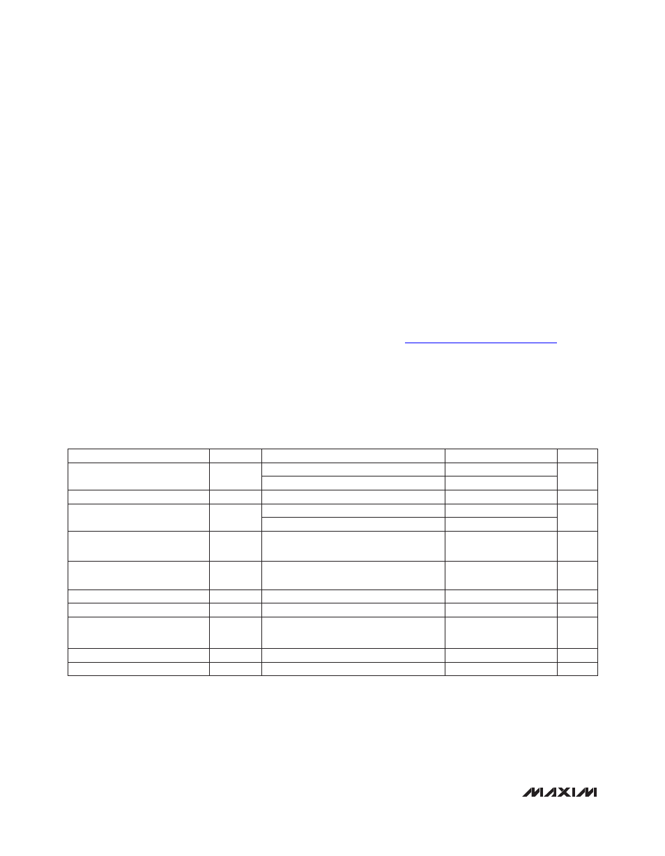
PARAMETER
SYMBOL
CONDITIONS
MIN
TYP
MAX
UNITS
Supply Voltage Range
V
IN
Continuous
3.5
30
V
For P 400ms
45
Supply Current
I
LOAD
= 0, SET = GND, V
OUT
= 5V
20
30
F
A
Shutdown Supply Current
I
SHDN
ENABLE = GND, T
A
= +25NC
1.6
3
F
A
ENABLE = GND, -40NC P T
A
P +125NC
3
Output Voltage
(5V Fixed Output Setting)
V
OUT50
1mA P I
LOAD
P 200mA,
V
IN
= 6V to 30V (Note 3)
4.9
5.0
5.1
V
Output Voltage
(3.3V Fixed Output Setting)
V
OUT33
1mA P I
LOAD
P 200mA, V
IN
= 4.8V to 30V
(Note 3)
3.234
3.3
3.366
V
Adjustable Output-Voltage Range
V
OUT
1.5
11.0
V
SETOV FB Voltage
V
SETOV
I
LOAD
= 1mA
1.225
1.25
1.275
V
Dropout Voltage (Note 4)
D
V
DO
I
LOAD
= 200mA, SET = GND, SETOV =
HIGH, V
OUT(NORM)
= +5.0V
280
600
mV
Short-Circuit Output Current Limit
I
SC
Output shorted to GND (MAX16910C__)
230
330
mA
Thermal Shutdown
(Note 5)
+180
N
C
ELECTRICAL CHARACTERISTICS
(V
IN
= V
ENABLE
= +14V, C
TIMEOUT
= open, C
IN
= 1µF, C
OUT
= 4.7µF, unless otherwise noted. T
A
= T
J
= -40°C to +125°C, unless
otherwise noted. Typical values are T
A
= +25°C.) (Note 2)