Rainbow Electronics MAX16910 User Manual
Page 12

200mA, Automotive, Ultra-Low
Quiescent Current, Linear Regulator
MAX16910
12 _____________________________________________________________________________________
After determining the allowable power dissipation, cal-
culate the maximum allowable output current, without
exceeding the +150°C junction temperature, using the
following formula:
D
OUT(MAX)
IN
OUT
P
I
V
V
=
−
The above equations do not include the negligible power
dissipation from self-heating due to the device ground
current.
Example 1 (TDFN-EP Package):
T
A
= +125°C, V
IN
= 16V, V
OUT
= 3.3V
Calculate the maximum allowable power dissipation at
the given temperature as follows:
(
)
D
W
P
1.951W 0.0244
125 C 70 C 609mW
C
=
−
×
° −
°
=
°
And establish the maximum output current:
OUT(MAX)
609mW
I
48mA
16V 3.3V
=
≅
−
Example 2 (TDFN-EP Package):
T
A
= +50°C, V
IN
= 9V, V
OUT
= 5V
Calculate the maximum allowable power dissipation at
the given temperature as follows:
P
D
= 1.951W
Find the maximum output current:
OUT(MAX)
OUT(MAX)
SC
1.951W
I
488mA
I
I
= 330mA (typ)
9V 5V
=
=
⇒
=
−
In Example 2, the maximum output current is calculated
as 488mA. The allowable output current cannot exceed
the given internal current limit for the device of 330mA
(typ).
Selecting Timeout Capacitor
The reset timeout period is adjustable to accommodate
a variety of microprocessor applications. Adjust the
reset timeout period by connecting a capacitor between
TIMEOUT and GND.
RP
TO
TIMEOUT
1.25 C
t
I
×
=
where t
RP
is in ms and C
TIMEOUT
is in nF.
Leave TIMEOUT unconnected to select the internally
fixed timeout period. C
TIMEOUT
must be a low-leakage
(< 10nA) type capacitor. Ceramic capacitors are recom-
mended; do not use capacitor values lower than 100pF
to avoid the influence of parasitic capacitances.
Exposed Pad
The MAX16910 package features an exposed thermal
pad on its underside that should be used as a heatsink.
This pad lowers the package’s thermal resistance by
providing a direct heat-conduction path from the die
to the PCB. Connect the exposed pad and GND to the
system ground using a large pad or ground plane, or
multiple vias to the ground plane layer.
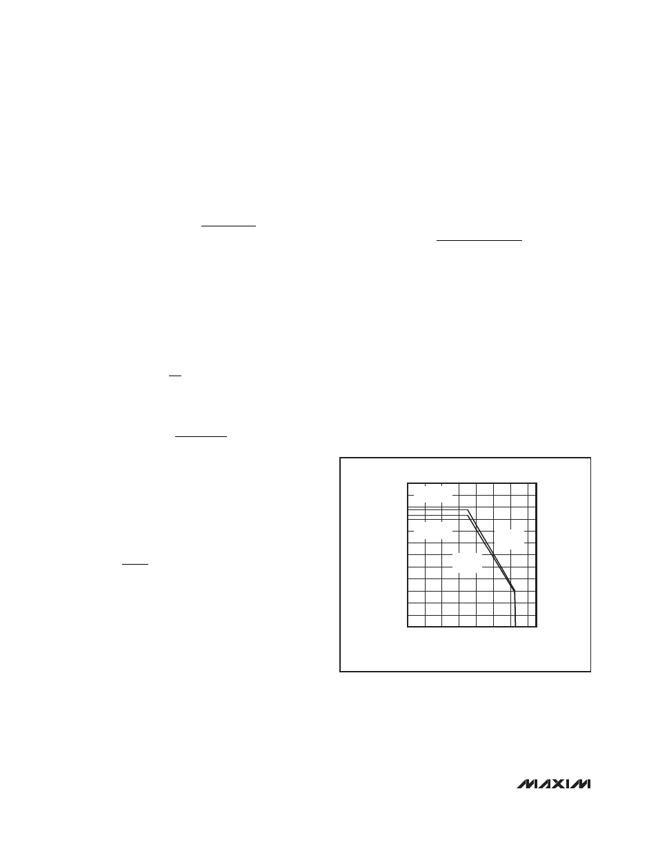
Figure 1. Calculated Maximum Power Dissipation vs. Ambient
Temperature
0
0.2
0.4
0.6
0.8
1.0
1.2
1.4
1.6
1.8
2.0
2.2
2.4
0
20
40
60
80
100
120
140
TEMPERATURE (°C)
P
D
(W)
1.951W
8-PIN TDFN-EP
1.861W
8-PIN SO-EP
DERATE
24.4mW/°C
DERATE
23.3mW/°C
