Rainbow Electronics MAX9101 User Manual
Page 2
MAX9100/MAX9101
+1.0V Micropower SOT23 Comparators
2
_______________________________________________________________________________________
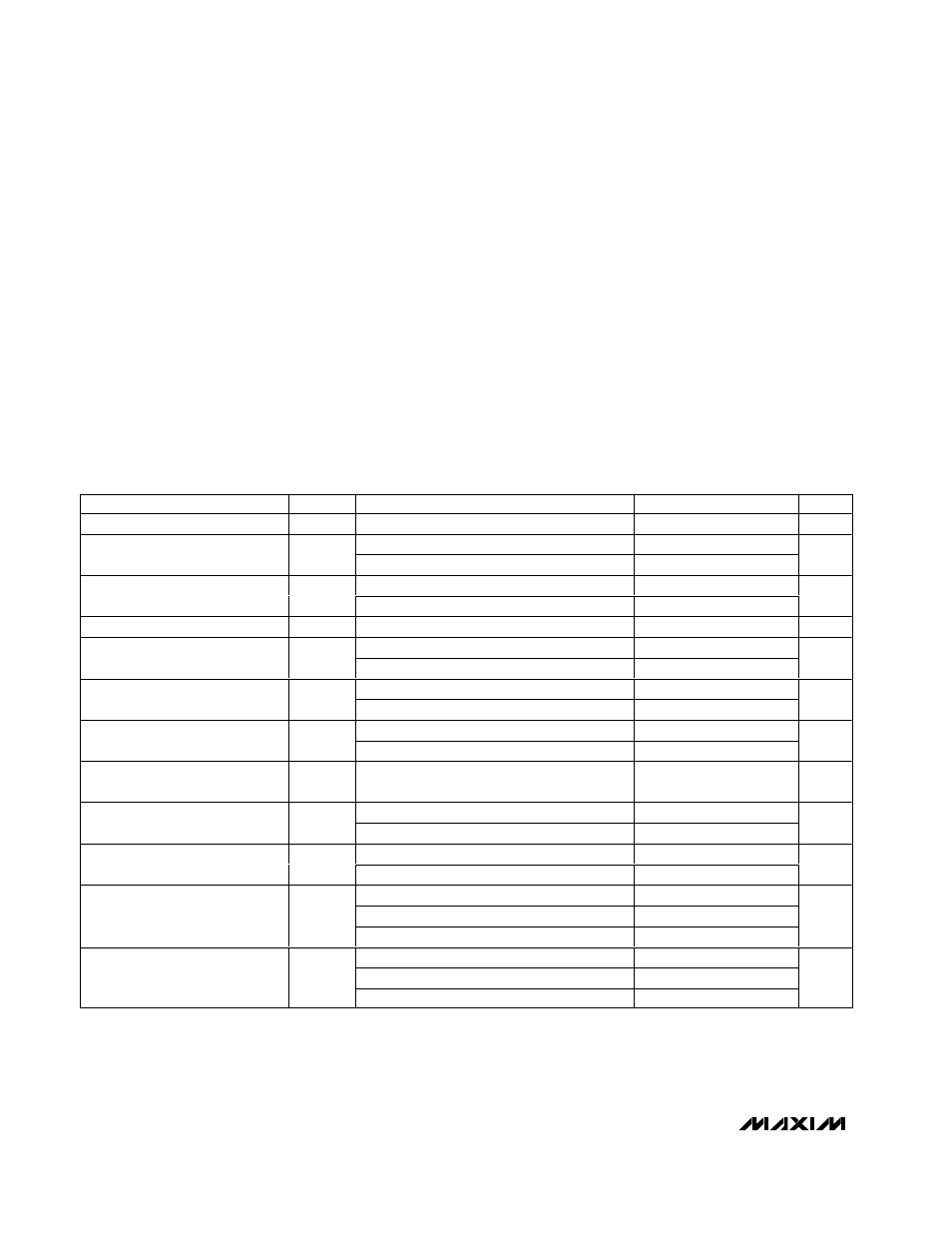
ABSOLUTE MAXIMUM RATINGS
ELECTRICAL CHARACTERISTICS
(V
CC
= +1.2V to +5.5V, V
CM
= 0, and T
A
= T
MIN
to T
MAX
, unless otherwise noted. Typical values are at T
A
= +25
°C.) (Note 1)
Stresses beyond those listed under “Absolute Maximum Ratings” may cause permanent damage to the device. These are stress ratings only, and functional
operation of the device at these or any other conditions beyond those indicated in the operational sections of the specifications is not implied. Exposure to
absolute maximum rating conditions for extended periods may affect device reliability.
Supply Voltage (V
CC
to GND) ................................. -0.3V to +6V
IN+ or IN- to GND...................................... -0.3V to (V
CC
+ 0.3V)
Output Voltages to GND
MAX9100 .............................................. -0.3V to (V
CC
+ 0.3V)
MAX9101 ............................................................ -0.3V to +6V
Output Short-Circuit Duration (to V
CC
or GND)......... Continuous
Continuous Power Dissipation (T
A
= +70
°C)
5-Pin Plastic SOT23
(derate 7.3mW/
°C above +70°C)............................... 571mW
8-Pin Plastic SO
(derate 5.88mW/
°C above +70°C)............................. 471mW
Operating Temperature Range .......................... -40
°C to +85°C
Junction Temperature ..................................................... +150
°C
Storage Temperature Range ............................ -65
°C to +150°C
Lead Temperature (soldering, 10s) .................................+300°C
PARAMETER
SYMBOL
CONDITIONS
MIN
TYP
MAX
UNITS
Supply Voltage Range
V
CC
Inferred from the PSRR tests
1.0
5.5
V
V
CC
= +1V, T
A
= +25
°C
5.0
8.0
Supply Current
I
CC
V
CC
= +5V, T
A
= T
MIN
to T
MAX
6.0
13.0
µA
T
A
= +25
°C
±3
±10
Input Offset Voltage
V
OS
T
A
= T
MIN
to T
MAX
±20
mV
Input Hysteresis
V
HYST
±2
mV
V
CC
= +5.5V, T
A
= +25
°C
±0.1
±5
Input Offset Current
I
OS
V
CC
= +5.5V, T
A
= T
MIN
to T
MAX
±10
nA
V
CC
= +5.5V, T
A
= +25
°C
±5
±15
Input Bias Current
I
B
V
CC
= +5.5V, T
A
= T
MIN
to T
MAX
±30
nA
Differential mode
200
Input Resistance
R
IN
Common mode
65
M
Ω
Input Common-Mode Voltage
Range (Note 2)
V
CM
Inferred from CMRR test
0
V
C C
- 0.2
V
T
A
= +25
°C
54
68
Common-Mode
Rejection Ratio (Note 3)
CMRR
T
A
= T
MIN
to T
MAX
46
dB
1.0V
≤ V
CC
≤ 1.5V, T
A
= +25
°C
54
66
Power-Supply
Rejection Ratio
PSRR
1.5V
≤ V
CC
≤ 5.5V, T
A
= -40
°C to +85°C
56
68
dB
V
CC
= +5.0V, I
SOURCE
= 5mA
90
180
V
CC
= +1.2V, I
SOURCE
= 0.5mA
60
120
Output Voltage High (MAX9100)
V
C C
- V
OH
V
CC
= +1.0V, I
SOURCE
= 0.1mA, T
A
=
25
75
mV
V
CC
= +5.0V, I
SINK
= 5mA
100
180
V
CC
= +1.2V, I
SINK
= 0.5mA
45
120
Output Voltage Low
V
OL
V
CC
= +1.0V, I
SINK
= 0.5mA, T
A
= +25
°C
15
75
mV