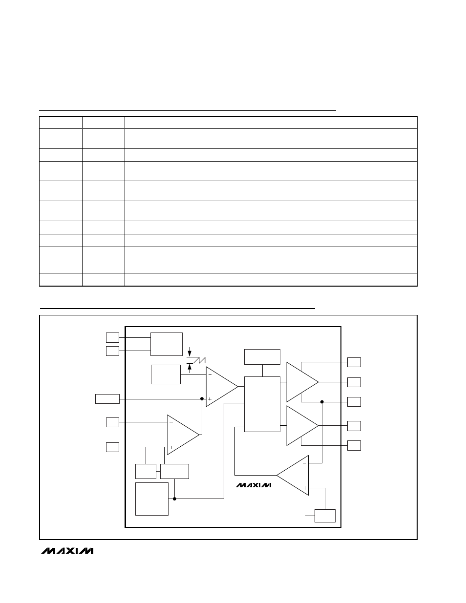
Pin description, Functional diagram – Rainbow Electronics MAX8548 User Manual
Page 7
MAX8545/MAX8546/MAX8548
Low-Cost, Wide Input Range, Step-Down
Controllers with Foldback Current Limit
_______________________________________________________________________________________
7
Pin Description
PIN
NAME
FUNCTION
1
COMP/EN
Compensation Input. Pull COMP/EN low with an open-collector or open-drain device to turn
off the output.
2
FB
Feedback Input. Connect a resistive-divider network to set V
OUT
. FB threshold is 0.8V.
3
V
CC
Internal Chip Supply. Connect V
CC
to VL through a 10
Ω resistor. Bypass V
CC
to GND with at
least a 0.1µF ceramic capacitor.
4
V
IN
Power Supply for LDO Regulator for V
IN
> 5.5V, and Chip Supply for V
IN
< 5.5V. Bypass V
IN
with
at least a 1µF ceramic capacitor to GND.
5
VL
Output of Internal 5V LDO. Connect VL to V
IN
for V
IN
< 5.5V. Bypass VL with at least a 1µF ceramic
capacitor to GND.
6
DL
Low-Side External MOSFET Gate-Driver Output. DL swings from VL to GND.
7
GND
Ground and Negative Current-Sense Input
8
LX
Inductor Switching Node. LX is used for both current limit and the return supply of the DH driver.
9
DH
High-Side External MOSFET Gate-Driver Output. DH swings from BST to LX.
10
BST
Positive Supply of DH Driver. Connect a 0.1µF ceramic capacitor between BST and LX.
V
IN
VL
FB
BST
DH
LX
V
CC
COMP/EN
5V LINEAR
REGULATOR
RAMP
GENERATOR
MAX8545
MAX8546
MAX8548
1V
PWM COMP
ERROR
AMPLIFIER
800mV
REF
SOFT-START
INTERNAL
CHIP SUPPLY
100kHz/
300kHz*
CLOCK
GENERATOR
*SEE SELECTOR GUIDE
CONTROL
LOGIC
TEMPERATURE
SHUTDOWN
DL
GND
FOLD-
BACK
FB
CURRENT-LIMIT
COMPARATOR
Functional Diagram