Rainbow Electronics MAX8548 User Manual
Page 14
MAX8545/MAX8546/MAX8548
Low-Cost, Wide Input Range, Step-Down
Controllers with Foldback Current Limit
14
______________________________________________________________________________________
ground terminals flush against one another. Follow these
guidelines for good PC board layout:
1) Keep the high-current paths short, especially at the
ground terminals. This practice is essential for sta-
ble, jitter-free operation.
2) Connect the power and analog grounds close to
the IC pin 7.
3) Keep the power traces and load connections short.
This practice is essential for high efficiency. Using
thick copper PC boards (2oz vs. 1oz) can enhance
full-load efficiency by 1% or more. Correctly routing
PC board traces is a difficult task that must be
approached in terms of fractions of centimeters,
where a few milohms of excess trace resistance
cause a measurable efficiency penalty.
4) LX and GND connections to the low-side MOSFET
for current sensing must be made using Kelvin
sense connections to guarantee the current-limit
accuracy. With SO-8 MOSFETs, this is best done
by routing power to the MOSFETs from outside
using the top copper layer, while connecting LX
and GND inside (underneath) the SO-8 package.
5) When tradeoffs in trace lengths must be made, it’s
preferable to allow the inductor charging current
path to be longer than the discharge path. For
example, it’s better to allow some extra distance
between the inductor and the low-side MOSFET or
between the inductor and the output filter capacitor.
6) Ensure that the connection between the inductor
and C3 is short and direct.
7) Route switching nodes (BST, LX, DH, and DL) away
from sensitive analog areas (COMP and FB).
Ensure the C1 ceramic bypass capacitor is immediately
adjacent to the pins and as close to the device as possi-
ble. Furthermore, the V
IN
and GND pins of MAX8545/
MAX8546/MAX8548 must terminate at the two ends of
C1 before connecting to the power switches and C2.
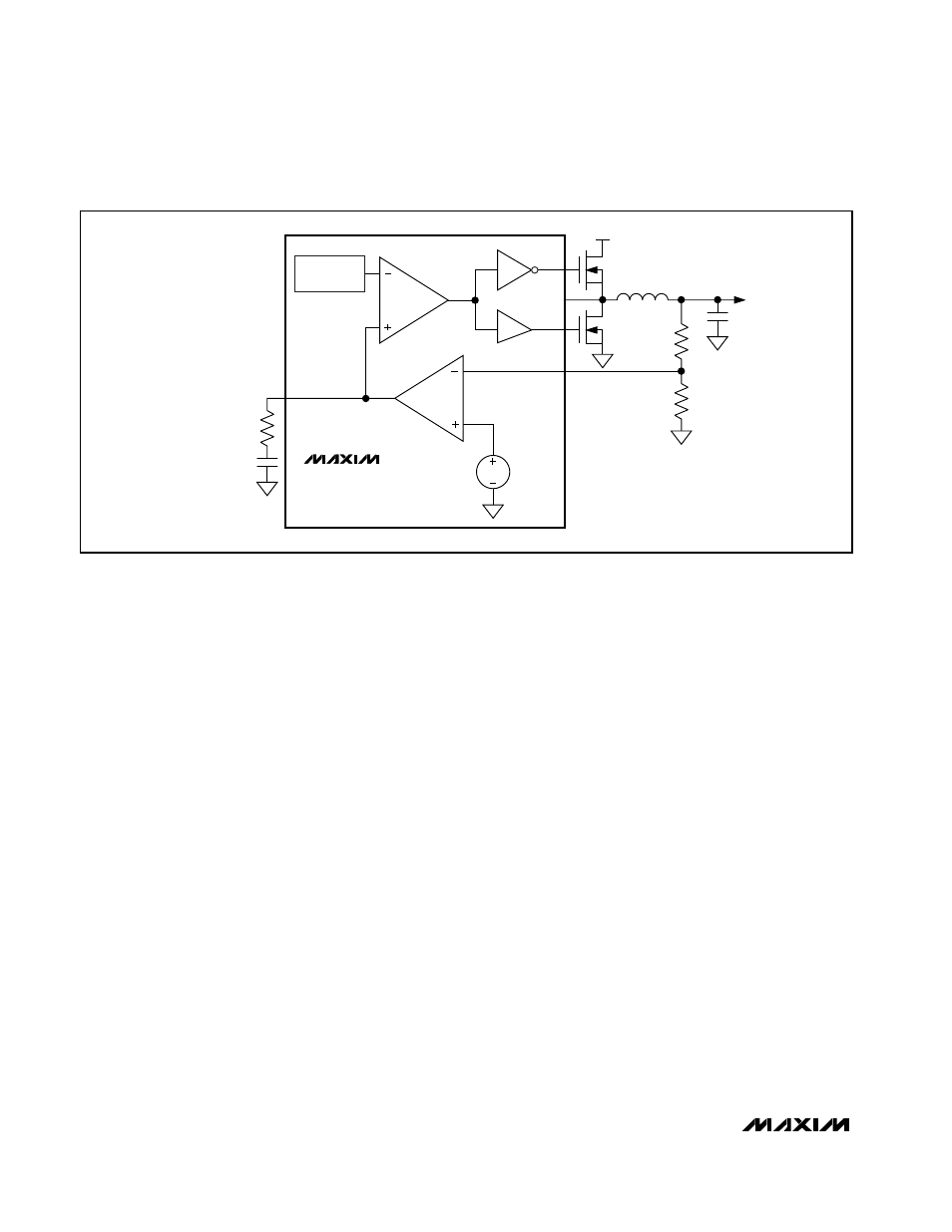
MAX8545
MAX8546
MAX8548
N
N
RAMP
GENERATOR
PWM
COMP/EN
R2
C10
C
OUT
V
OUT
R3
R4
L
V
IN
0.8V
ERROR
AMPLIFIER
DH
LX
DL
FB
Figure 3. Compensation Scheme