Pin configuration chip information, Package information – Rainbow Electronics MAX9937 User Manual
Page 10

MAX9937
Automotive Current-Sense Amplifier
with Reverse-Battery Protection
10
______________________________________________________________________________________
At frequencies below the output corner frequency, the
MAX9937 itself provides excellent 100dB (DC) com-
mon-mode rejection. At higher frequencies, as the
CMRR of the MAX9937 degrades, the output filter
formed by R
OUT
and C
OUT
helps boost the common-
mode rejection of the circuit.
Input Common-Mode Voltages
> 28V and < 0V
Short-duration overvoltages on the battery line are iso-
lated from the RSP and RSN pins of the MAX9937 by
the use of input resistors R
RSP
and R
RSN
. The input
ESD clamp structure is designed so that the device can
withstand short-duration (< 1s) overvoltages up to 40V
when using resistors R
RSP
and R
RSN
of 500
Ω or greater
as shown in the
Typical Application Circuit
.
Approximately 40mA flows out of each ESD diode dur-
ing this condition (20V/500
Ω). This current is less than
the 50mA absolute maximum specification for the RSN
and RSP pins.
Skewed Input Offset Voltage
for Production Calibration
Due to low temperature drift of input bias current and
input offset voltage in the MAX9937, the part can be
used to provide powerful application and system bene-
fits not normally attainable from other current-sense
amplifiers on the market. For example, input resistors
R
RSP
and R
RSN
can be intentionally mismatched so as
to introduce an external, controlled input offset voltage
into the circuit. Doing so allows microcontroller firmware
to trim out input offset voltages completely by using
production-line calibration during the manufacturing
process or in system operation as long as a zero load-
current condition is forced. Only minimal temperature-
drift-based errors in the resistor and in the bias currents
then remain.
V
OS-FINAL
= V
OS
+ I
B-
x R
RSN
- I
B+
x R
RSP
while gain = R
OUT
/R
RSP
.
Since gain can be fixed by choosing R
OUT
and R
RSP
, a
positive offset voltage can be induced by varying the
value of R
RSN
compared to R
RSP
.
For example:
R
OUT
= 10k
Ω, R
RSP
= 500
Ω fixes gain = 20V/V. Now,
choosing R
RSN
= 2.5k
Ω, and knowing ΔI
B
= ±12% of I
B
,
the additional V
OS
becomes:
ΔV
OS
(max) = (5.6µA x 2500) ± (0.12 x 5.6µA x 2500) -
(5.6µA x 500) = 11.2mV ± 1.7mV
ΔV
OS
(min) = (0.8µA x 2500) ± (0.12 x 0.8µA x 2500) -
(0.8µA x 500) = 1.6mV ± 0.24mV
Since the minimum extra V
OS
introduced into the part is
greater than the maximum V
OS
of the current-sense
amplifier (= 1mV), the output of the current-sense
amplifier is always greater than zero even at zero sense
voltage, thus allowing the current-sense amplifier to be
calibrated at zero input current.
Operation with V
CC
= 0V (Shutdown)
The input terminals go into a high-impedance mode
when V
CC
= 0, as shown by the input bias current in
shutdown 1µA specification. Due to the low 20µA sup-
ply current, this then becomes a convenient way to put
the amplifier in shutdown simply by using a digital I/O
port of a microcontroller to power up/down the current-
sense amplifier. This can be especially useful in certain
battery-operated applications that need to implement
flexible power-management schemes.
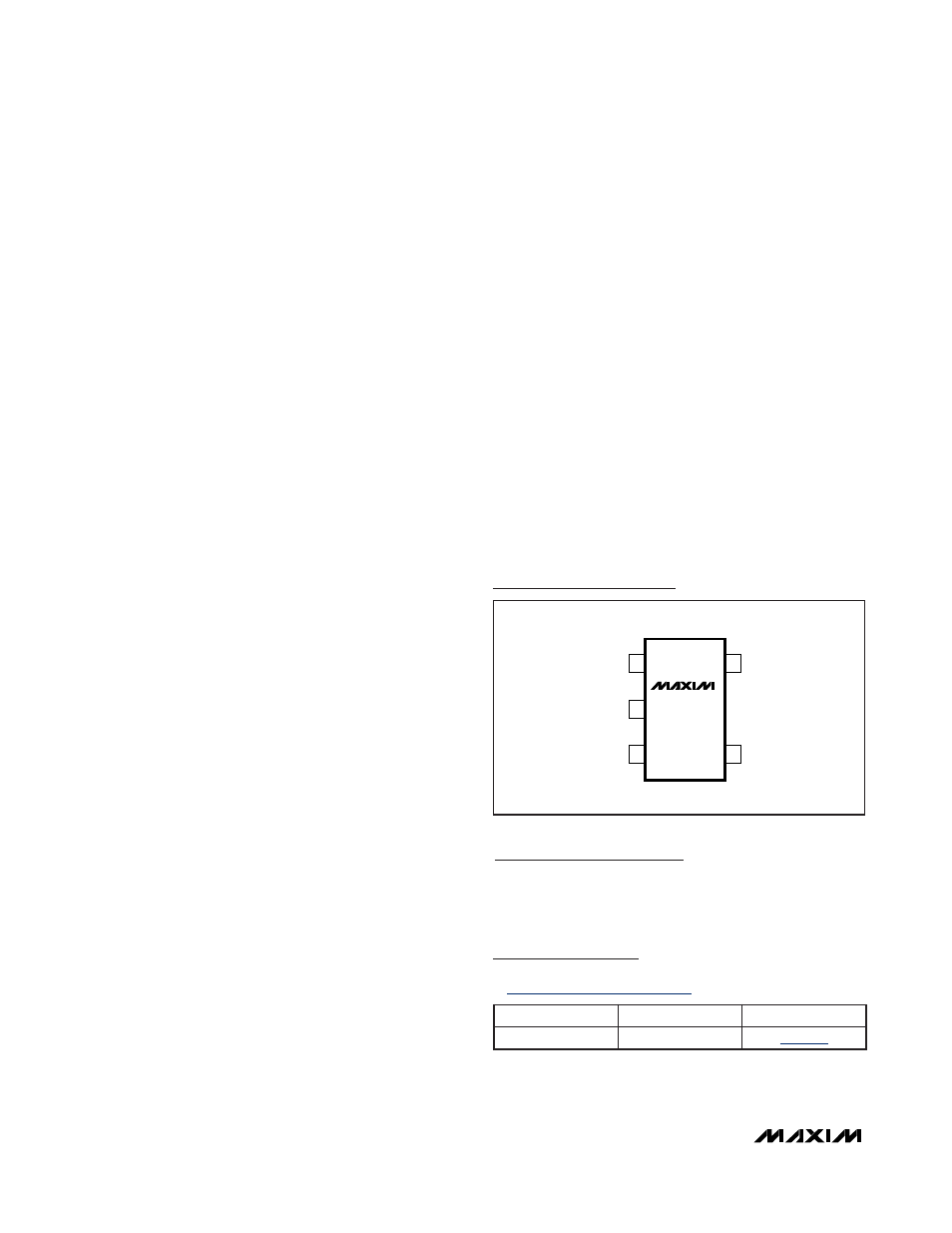
GND
RSN
OUT
1
5
RSP
V
CC
MAX9937
SC70
TOP VIEW
2
3
4
+
Pin Configuration
Chip Information
PROCESS: BiCMOS
Package Information
For the latest package outline information and land patterns, go
to
www.maxim-ic.com/packages
.
PACKAGE TYPE
PACKAGE CODE
DOCUMENT NO.
5 SC70
X5+1
