Rainbow Electronics MX7828 User Manual
Page 7
does not require microprocessor WAIT states. A READ
operation simultaneously initiates a conversion and
reads the previous conversion result.
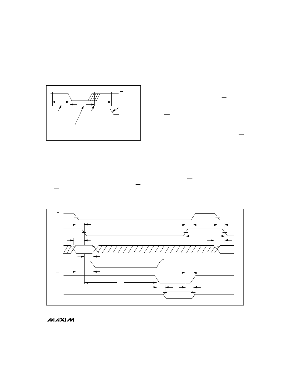
Interface Mode 0
Figure 5 shows the timing diagram for Mode 0 opera-
tion. This is used with microprocessors that have WAIT
state capability, whereby a READ instruction is extend-
ed to accommodate slow-memory devices. Taking CS
and RD low latches the analog multiplexer address and
starts a conversion. Data outputs DB0–DB7 remain in
the high-impedance condition until the conversion is
complete.
There are two status outputs: Interrupt (INT) and Ready
(RDY). RDY, an open-drain output (no internal pull-up
device), is connected to the processor’s READY/WAIT
input. RDY goes low on the falling edge of CS and goes
high impedance at the end of the conversion, when the
conversion result appears on the data outputs. If the RDY
output is not required, its external pull-up resistor can be
omitted. INT goes low when the conversion is complete
and returns high on the rising edge of CS or RD.
Interface Mode 1
Mode 1 is designed for applications where the micro-
processor is not forced into a WAIT state. Taking CS
and RD low latches the multiplexer address and starts
a conversion (Figure 6). Data from the previous conver-
sion is immediately read from the outputs (DB0–DB7).
INT goes high at the rising edge of CS or RD and goes
low at the end of the conversion. A second READ oper-
ation is required to read the result of this conversion.
The second READ latches a new multiplexer address
and starts another conversion. A delay of 2.5µs must
be allowed between READ operations. RDY goes low
on the falling edge of CS and goes high impedance at
the rising edge of CS. If RDY is not needed, its external
pull-up resistor can be omitted.
MX7824/MX7828
CMOS, High-Speed, 8-Bit ADCs
with Multiplexer
_______________________________________________________________________________________
7
500ns
V
IN
IS TRACKED
BY INTERNAL
COMPARATORS
V
IN
IS SAMPLED
AND THE FOUR MSBs
ARE LATCHED
SETUP TIME REQUIRED
BY THE INTERNAL
COMPARATORS PRIOR TO
STARTING CONVERSION
600ns
RD
INT GOING LOW
INDICATES THAT
CONVERSION IS
COMPLETE AND
THAT DATA CAN
BE READ
1000ns
Figure 4. Operating Sequence
DATA
DATA
VALID
ADDR
VALID
ADDR
VALID
INT
RDY
RD
ANALOG
CHANNEL
ADDRESS
CS
t
AS
t
AH
t
RDY
t
CRD
HIGH IMPEDANCE
t
CSS
t
CSS
t
INTH
t
DH
t
ACC2
t
AS
t
P
t
CSH
Figure 5. Mode 0 Timing Diagram