Pin descriptions – Rainbow Electronics MX7828 User Manual
Page 5
MX7824/MX7828
CMOS, High-Speed, 8-Bit ADCs
with Multiplexer
_______________________________________________________________________________________
5
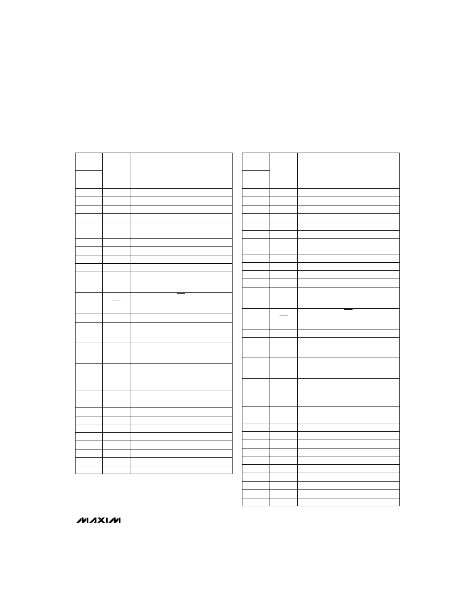
Reference Output (2.5V) for MAX154.
Test point for MX7824. Do not connect.
REF OUT
TP
5
Three-State Data Output, bit 0 (LSB)
DBO
6
Three-State Data Output, bit 1
DB1
7
Analog Input Channel 1
AIN1
4
Analog Input Channel 2
AIN2
3
PIN
Analog Input Channel 3
AIN3
2
Analog Input Channel 4
AIN4
1
FUNCTION
NAME
_____________________________________________________________Pin Descriptions
Three-State Data Output, bit 2
DB2
8
Three-State Data Output, bit 3
DB3
9
Read Input.
–
R
—
D
–
controls conversions
and data access. See
Digital Interface
section.
–
R
—
D
–
10
Three-State Data Output, bit 7 (MSB)
DB7
20
Ground
GND
12
Lower Limit of Reference Span. Sets
the zero-code voltage.
Range: GND to V
REF
+.
V
REF
-
13
Interrupt Output. INT going low indi-
cates the completion of a conversion.
See
Digital Interface
section.
INT
11
Chip-Select Input.
–
C
—
S
–
must be low for
the device to be selected.
–
C
—
S
–
16
Three-State Data Output, bit 4
DB4
17
Three-State Data Output, bit 5
DB5
18
Three-State Data Output, bit 6
DB6
19
Interrupt Output. INT going low indi-
cates the completion of a conversion.
See
Digital Interface
section.
INT
13
Ground
GND
14
Analog Input Channel 2
AIN2
5
Analog Input Channel 1
AIN1
6
Reference Output (2.5V) for MAX158.
Test point for MX7828. Do not connect.
REF OUT
TP
7
Analog Input Channel 3
AIN3
4
Analog Input Channel 4
AIN4
3
PIN
Analog Input Channel 5
AIN5
2
Analog Input Channel 6
AIN6
1
FUNCTION
NAME
Three-State Data Output, bit 0 (LSB)
DB0
8
Three-State Data Output, bit 1
DB1
9
Three-State Data Output, bit 2
DB2
10
Three-State Data Output, bit 3
DB3
11
Lower Limit of Reference Span. Sets
the zero-code voltage.
Range: GND to V
REF
+.
V
REF
-
15
Read Input.
–
R
—
D
–
controls conversions
and data access. See
Digital Interface
section.
–
R
—
D
–
12
Ready Output. Open-drain output with
no active pull-up device. Goes low
when
–
C
—
S
–
goes low and high imped-
ance at the end of a conversion.
RDY
17
Power-Supply Voltage, +5V
V
DD
26
Channel Address 2 Input
A2
23
Channel Address 1 Input
A1
24
Channel Address 0 Input
A0
25
Upper Limit of Reference Span. Sets
the full-scale input voltage.
Range: V
REF
- to V
DD
.
V
REF
+
14
Ready Output. Open-drain output with
no active pull-up device. Goes low
when
–
C
—
S
–
goes low and high imped-
ance at the end of a conversion.
RDY
15
Power-Supply Voltage, +5V
V
DD
24
Channel Address 1 Input
A1
21
Channel Address 0 Input
A0
22
No Connect
NC
23
Three-State Data Output, bit 7 (MSB)
DB7
22
Chip-Select Input.
–
C
—
S
–
must be low for
the device to be selected.
–
C
—
S
–
18
Three-State Data Output, bit 4
DB4
19
Three-State Data Output, bit 5
DB5
20
Three-State Data Output, bit 6
DB6
21
Analog Input Channel 8
AIN8
27
Analog Input Channel 7
AIN7
28
Upper Limit of Reference Span. Sets
the full-scale input voltage.
Range: V
REF
- to V
DD
.
V
REF
+
16
MAX154
MX7824
MAX158
MX7828