Detailed description, Digital interface, Table 1. truth table for input channel selection – Rainbow Electronics MX7828 User Manual
Page 6
MX7824/MX7828
CMOS, High-Speed, 8-Bit ADCs
with Multiplexer
6
_______________________________________________________________________________________
_______________Detailed Description
Converter Operation
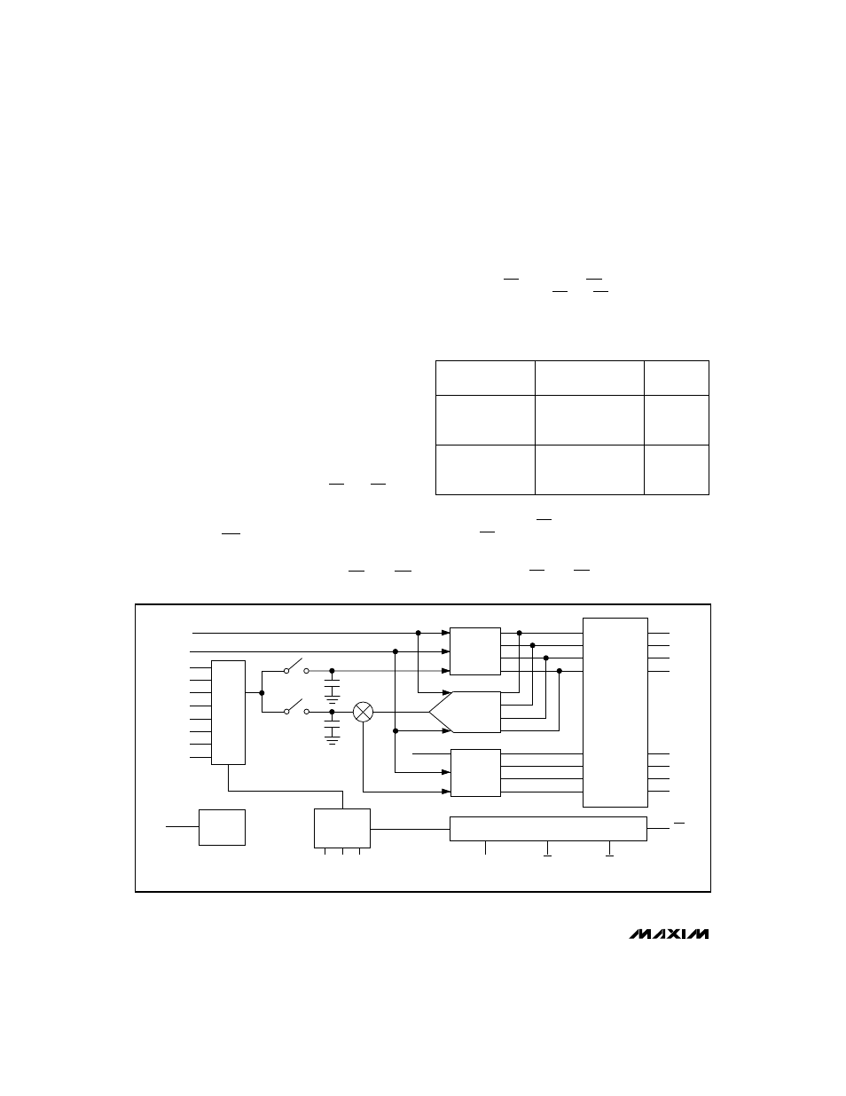
The MAX154/MAX158 and MX7824/MX7828 use what is
commonly called a “half-flash” conversion technique
(Figure 3). Two 4-bit flash ADC sections are used to
achieve an 8-bit result. Using 15 comparators, the
upper 4-bit MS (most significant) flash ADC compares
the unknown input voltage to the reference ladder and
provides the upper four data bits.
An internal DAC uses the MS bits to generate an analog
signal from the first flash conversion. A residue voltage
representing the difference between the unknown input
and the DAC voltage is then compared to the reference
ladder by 15 LS (least significant) flash comparators to
obtain the lower four output bits.
Operating Sequence
The operating sequence is shown in Figure 4. A con-
version is initiated by a falling edge of RD and CS. The
comparator inputs track the analog input voltage for
approximately 1µs. After this first cycle, the MS flash
result is latched into the output buffers and the LS con-
version begins. INT goes low approximately 600ns
later, indicating the end of the conversion, and that the
lower four bits are latched into the output buffers. The
data can then be accessed using the CS and RD
inputs.
___________________Digital Interface
The MAX154/MAX158 and MX7824/MX7828 use only
Chip Select (CS) and Read (RD) as control inputs. A
READ operation, taking CS and RD low, latches the mul-
tiplexer address inputs and starts a conversion (Table 1).
There are two interface modes, which are determined
by the length of the RD input. Mode 0, implemented by
keeping RD low until the conversion ends, is designed
for microprocessors that can be forced into a WAIT
state. In this mode, a conversion is started with a READ
operation (taking CS and RD low), and data is read
when the conversion ends. Mode 1, on the other hand,
4-BIT
DAC
THREE-
STATE
DRIVERS
ADDRESS
LATCH
DECODE
4-BIT
FLASH
ADC
(4LSB)
4-BIT
FLASH
ADC
(4MSB)
2.5V
REF
TIMING AND CONTROL
CIRCUITRY
MUX*
V
REF
+
V
REF
+
16
A0
*MAX154/MX7824 – 4-Channel Mux
MAX158/MX7828 – 8-Channel Mux
** REF OUT on MAX154/MAX158 only
A1
A2
RDY
CS
RD
AIN1
AIN4
AIN8
REF OUT**
V
REF
-
DB7
DB6
DB5
DB4
DB3
DB2
DB1
DB0
INT
MAX154/MX7824
A1
A0
MAX158/MX7828
A2
A1
A0
SELECTED
CHANNEL
0
0
0
1
1
0
1
1
0
0
0
0
0
1
0
1
0
0
1
1
AIN1
AIN2
AIN3
AIN4
Figure 3. Functional Diagram
Table 1. Truth Table for Input Channel
Selection
1
0
0
1
0
1
1
1
0
1
1
1
AIN5
AIN6
AIN7
AIN8