Rainbow Electronics MAX11043 User Manual
Page 29
MAX11043
4-Channel, 16-Bit, Simultaneous-Sampling ADCs
with PGA, Filter, and 8-/12-Bit Dual-Stage DAC
______________________________________________________________________________________
29
Flash Erase and Programming
When erasing or programming the flash, maintain the
system clock between 14MHz and 27MHz to satisfy
flash timing requirements and ensure CONVRUN = 0.
The system clock used for all digital timing is twice the
ADC sample clock (2 x EX clock/divider).
Always erase the flash page before writing new data.
The procedure for flash mass erase is as follows:
1) Read the flash mode register (18h); proceed when
the LSB is zero.
2) Write 0000h to the flash address register (19h).
3) Write 60h to the flash mode register (18h).
4) Wait 200ms for erase to complete.
5) FFFFh = flash erased state.
The procedure for flash single page erase is as follows:
1) Read the flash mode register (18h); proceed when
the LSB is zero.
2) Write page address, set word address to 00h in the
flash address register (19h).
3) Write 40h to the flash mode register (18h).
4) Wait 20ms for page erase to complete.
5) FFFFh = flash erased state.
The procedure for flash single word write is as follows:
1) Read the flash mode register (18h); proceed when
the LSB is zero.
2) Write page and word address to the flash address
register (19h).
3) Write the data to the flash data in register (1Ah).
4) Write 20h to the flash mode register (18h).
5) Read the flash mode register (18h); proceed when
the LSB is zero (approx. 40µs).
The procedure for flash single word read is as follows:
1) Read the flash mode register (18h); proceed when
the LSB is zero.
2) Write page and word address to the flash address
register (19h).
3) Write 80h to the flash mode register (18h).
4) Read the flash mode register (18h); proceed when
the LSB is zero (approx. 1µs).
5) Read the data from the flash data out register (1Bh).
The procedure for flash to C-RAM transfer is as follows:
1) Read the flash mode register (18h); proceed when
the LSB is zero.
2) Write A0h to the flash mode register (18h).
3) Read the flash mode register (18h); proceed when
the LSB is zero (approx. 1ms).
4) The content of flash is transferred to C-RAM.
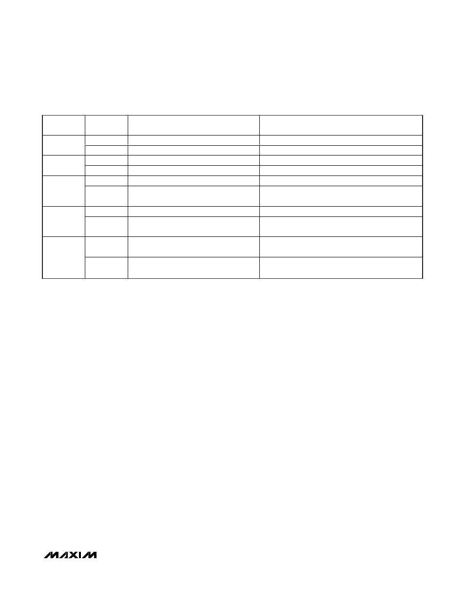
C-RAM
ADDRESS
FLASH
ADDRESS
MSB FOR C-RAM
LSB FOR C-RAM
76h
—
Not used
3Bh
77h*
ADC gain trim for gain = 32
—
78h
—
Not used
3Ch
79h*
ADC gain trim for gain = 64
—
7Ah*
—
LP filter gain for filter stage 1, gain = 8
3Dh
7Bh*
LP filter coefficient A2 for filter stage 1,
gain = 8
—
7Ch
—
Not used
3Eh
7Dh*
LP filter coefficient A3 for filter stage 1,
gain = 8
—
7Eh*
—
LP filter coefficient B3 and rectify bit for filter stage 1,
gain = 8
3Fh
7Fh*
LP filter coefficient B2 for filter stage 1,
gain = 8
—
Table 3. C-RAM and Flash Memory Map (continued)
*
Recommended copy to C-RAM or flash for optimum custom-filter performance.