Absolute maximum ratings – Rainbow Electronics MAX9013 User Manual
Page 2
MAX9010–MAX9013
SC70, 5ns, Low-Power, Single-Supply,
Precision TTL Comparators
2
_______________________________________________________________________________________
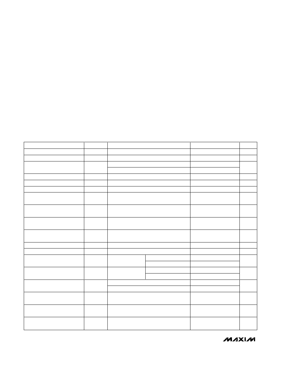
ABSOLUTE MAXIMUM RATINGS
Stresses beyond those listed under “Absolute Maximum Ratings” may cause permanent damage to the device. These are stress ratings only, and functional
operation of the device at these or any other conditions beyond those indicated in the operational sections of the specifications is not implied. Exposure to
absolute maximum rating conditions for extended periods may affect device reliability.
Power Supply (V
CC
to GND) ...................................-0.3V to +6V
Analog Input (IN+ or IN-) to GND...............-0.3V to (V
CC
+ 0.3V)
Input Current (IN+ or IN-) .................................................±30mA
LE to GND ..................................................-0.3V to (V
CC
+ 0.3V)
Continuous Output Current...............................................±40mA
Continuous Power Dissipation (T
A
= +70°C)
6-Pin SC70 (derate 3.1mW/°C above +70°C) .............245mW
6-Pin SOT23 (derate 8.7mW/°C above +70°C)...........696mW
8-Pin µMAX (derate 4.5mW/°C above +70°C) ............362mW
8-Pin SO (derate 5.9mW/°C above +70°C).................471mW
Operating Temperature Range ...........................-40°C to +85°C
Junction Temperature ......................................................+150°C
Storage Temperature Range .............................-65°C to +150°C
Lead Temperature (soldering, 10s) .................................+300°C
ELECTRICAL CHARACTERISTICS (MAX9010/MAX9011)
(V
CC
= 5V, V
LE
= 0 (MAX9011 only), V
CM
= 0, T
A
= T
MIN
to T
MAX
, unless otherwise noted. Typical values are at T
A
= +25°C.) (Note 1)
PARAMETER
SYMBOL
CONDITIONS
MIN
TYP
MAX
UNITS
Supply Voltage Range
V
CC
Inferred from V
OS
tests
4.5
5.5
V
Power-Supply Current (Note 2)
I
CC
0.90
2.1
mA
T
A
= +25°C
±1
±5
Input Offset Voltage
(Note 3)
V
OS
T
A
=
T
MIN
to T
MAX
±7
mV
Input Offset-Voltage Drift
∆V
OS/
∆T
±2
µV /°C
Input Bias Current
I
B
±0.5
±2
µA
Input Offset Current
I
OS
±40
±200
nA
Differential Input Resistance
(Note 4)
R
IN (D IFF)
V
IN(DIFF)
= ±10mV
250
k
Ω
Common-Mode Input
Resistance (Note 4)
R
IN(CM)
-0.2V
≤ V
CM
≤ (V
CC
- 1.9V)
1
M
Ω
Common-Mode Input Voltage
Range (Note 4)
V
CM
Inferred from V
OS
tests
-0.2
V
CC
- 1.9
V
Common-Mode Rejection
Ratio
CMRR
-0.2V
≤ V
CM
≤ (V
CC
- 1.9V)
95
dB
Power-Supply Rejection Ratio
PSRR
V
CC
= 4.5V to 5.5V
82
dB
Small-Signal Voltage Gain
A
V
1V
≤ V
OUT
≤ 2V
3000
V/V
I
SINK
= 0
0.3
0.5
Output Low Voltage
V
OL
V
IN
≥ 100mV
I
SINK
= 4mA
0.5
0.6
V
I
SOURCE
= 0
2.7
3.3
Output High Voltage
V
OH
V
IN
≥ 100mV,
V
CC
= 4.5V
I
SOURCE
= 4mA
2.4
2.9
V
Sinking
20
Output Short-Circuit Current
I
OUT
Sourcing
30
mA
Latch Enable Pin High Input
Voltage
V
IH
MAX9011 only
2
V
Latch Enable Pin Low Input
Voltage
V
IL
MAX9011 only
0.8
V
Latch Enable Pin Bias Current
I
IH
, I
IL
MAX9011 only,
V
LE
= 0 and V
LE
= 5V
±25
µA