Max5172 – Rainbow Electronics MAX5172 User Manual
Page 9
MAX5170/MAX5172
Low-Power, Serial, 14-Bit DACs
with Voltage Output
_______________________________________________________________________________________
9
-30
-20
-25
-10
-15
0
-5
5
0
1000
1500
500
2000
2500
3000
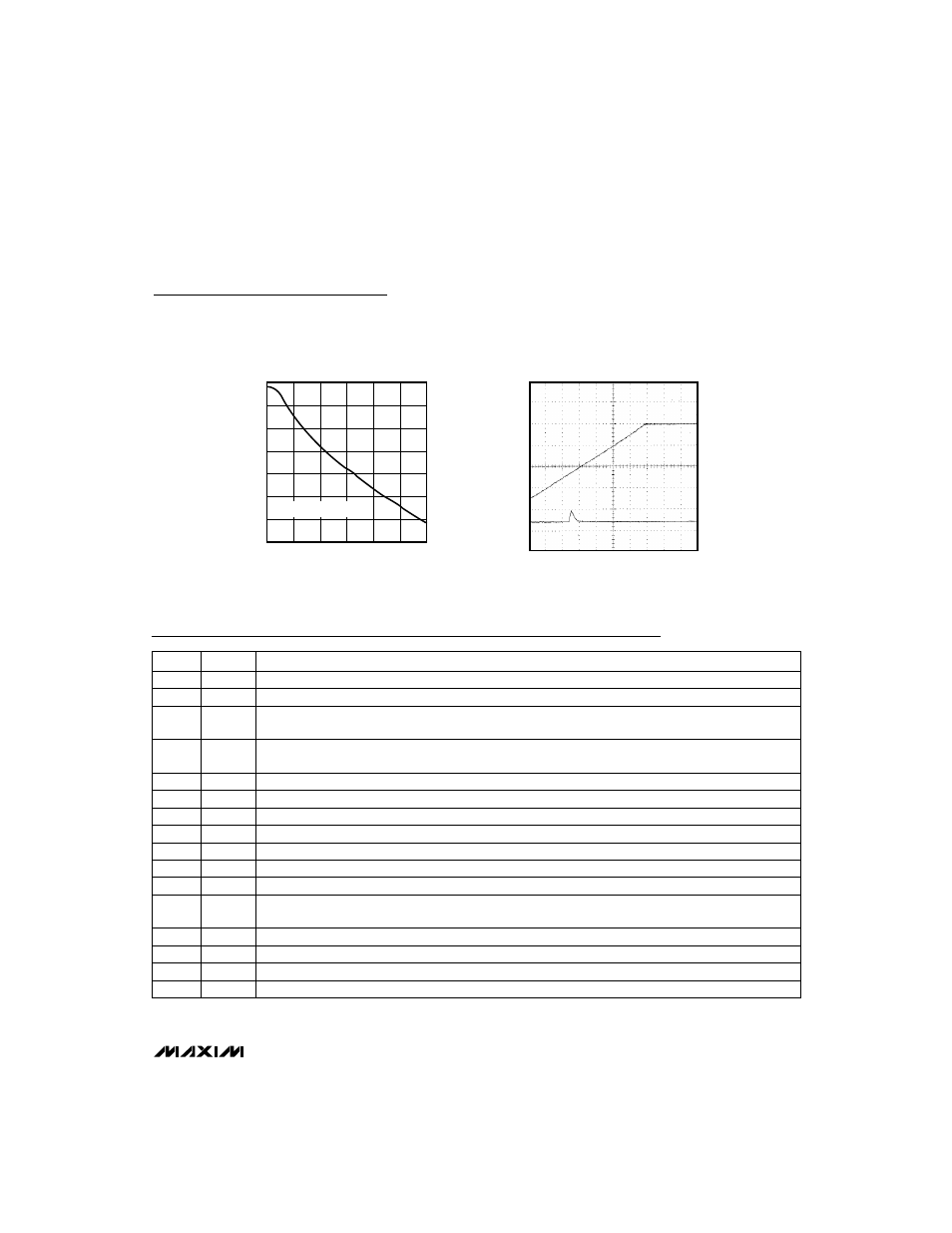
REFERENCE INPUT FREQUENCY RESPONSE
MAX5170/72 toc27
FREQUENCY (kHz)
GAIN (dB)
V
REF
= 0.67Vp-p + 0.75V
DC
V
DD
1V/div
V
OUT
10mV/div
START-UP GLITCH
MAX5170/72 toc28
50ms/div
AC-COUPLED
MAX5172
9
DGND
Digital Ground
13
AGND
Analog Ground
15
N.C.
No Connection
NAME
FUNCTION
1
OS
Offset Adjustment. Connect to AGND for no offset.
16
V
DD
Positive Supply. Bypass to AGND with a 4.7µF capacitor in parallel with a 0.1µF capacitor.
PIN
14
REF
Reference Input. Maximum V
REF
is V
DD
- 1.4V.
11
UPO
User-Programmable Output. State is set by the serial input.
12
SHDN
Shutdown (digital input). Pulling SHDN high when
PDL = V
DD
places the chip in shutdown with a maximum
shutdown current of 10µA.
10
DOUT
Serial-Data Output
5
CLR
Clear DAC (digital input). Clears the DAC to either zero or midscale as determined by RS.
7
DIN
Serial-Data Input (digital input). Data is clocked in on the rising edge of SCLK.
8
SCLK
Serial Clock Input (digital input)
6
CS
Chip Select Input (digital input). DIN ignored when
CS is high.
3
RS
Reset Mode Select (digital input). Connect to V
DD
to select midscale reset output voltage. Connect to
DGND to select 0 reset output voltage.
4
PDL
Power-Down Lockout (digital input). Connect to V
DD
to allow shutdown. Connect to DGND to disable
software and hardware shutdown.
2
OUT
Voltage Output. High impedance when in shutdown. The output voltage is limited to V
DD
.
Pin Description
Typical Operating Characteristics (continued)
(MAX5170: V
DD
= +5V, V
REF
= 2.5V; MAX5172: V
DD
= +3V, V
REF
= 1.25V; C
L
= 100pF, OS = GND, code = 3FFF hex,
T
A
= +25°C, unless otherwise noted.)