Detailed description – Rainbow Electronics MAX5172 User Manual
Page 10
MAX5170/MAX5172
Low-Power, Serial, 14-Bit DACs
with Voltage Output
10
______________________________________________________________________________________
Detailed Description
The MAX5170/MAX5172 14-bit, serial, voltage-output
DACs operate with a 3-wire serial interface. These
devices include a 16-bit shift register and a double-
buffered input composed of an input register and a
DAC register (see
Functional Diagram). In addition,
these devices employ a rail-to-rail output amplifier and
internally trimmed resistors to provide a gain of
+1.638V/V, maximizing the output voltage swing. The
MAX5170/MAX5172’s offset adjust pin allows for a DC
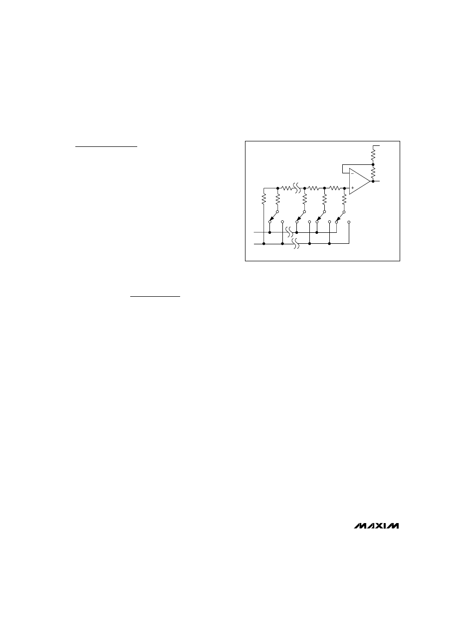
shift in the DAC output. The DACs are designed with an
inverted R-2R ladder network (Figure 1) which pro-
duces a weighted voltage proportional to the reference
voltage.
Reference Inputs
The reference input accepts both AC and DC values
with a voltage range extending from 0 to V
DD
- 1.4V.
The following equation represents the resulting output
voltage:
where N is the numeric value of the DAC’s binary input
code (0 to 16383), V
REF
is the reference voltage, and
Gain is the internal set voltage gain (+1.638V/V if OS =
AGND). The maximum output voltage is V
DD
. The refer-
ence pin has a minimum impedance of 18k
Ω
and is
code dependent.
Output Amplifier
With OS connected to AGND, the output amplifier
employs an internal, trimmed resistor-divider setting the
gain to +1.638V/V and minimizing gain error. The out-
put amplifier has a typical slew rate of 0.6V/µs and set-
tles to ±0.5LSB from a full-scale transition within 18µs,
when loaded with 5k
Ω
in parallel with 100pF. Loads
less than 2k
Ω
degrade performance.
For alternative output amplifier setups, refer to the
Applications Information section.
Shutdown Mode
The MAX5170/MAX5172 feature a software- and hard-
ware-programmable shutdown mode that reduces the
typical supply current to 1µA. Enter shutdown by writing
the appropriate input-control word as shown in Table 1
or by using the hardware shutdown. In shutdown mode,
the reference input and the amplifier output become
high-impedance and the serial interface remains active.
Data in the input register is saved, allowing the
MAX5170/MAX5172 to recall the prior output state
when returning to normal operation. Exit shutdown by
reloading the DAC register from the shift register, by
simultaneously loading the input and DAC registers, or
by toggling
PDL. When returning from shutdown, wait
40µs for the output to settle.
Power-Down Lockout
Power-Down Lockout disables the software/hardware
shutdown mode. A high-to-low transition brings the
device out of shutdown and returns the output to its
previous state.
Shutdown
Pulling SHDN high while
PDL is high places the
MAX5170/MAX5172 in shutdown. Pulling SHDN low will
not return the device to normal operation. A high-to-low
transition on
PDL or an appropriate command from the
serial data line (see Table 1 for commands) is required
to exit shutdown.
Serial-Interface
The MAX5170/MAX5172 3-wire serial interface is com-
patible with SPI, QSPI (Figure 2) and MICROWIRE
(Figure 3) interface standards. The 16-bit serial input
word consists of two control bits and 14 bits of data
(MSB to LSB).
The control bits determine the MAX5170/MAX5172’s
operation as outlined in Table 1. The MAX5170/
MAX5172’s digital inputs are double buffered, which
allows any of the following:
• Loading the input register without updating the DAC
register
• Updating the DAC register from the input register
• Updating the input and DAC registers simultaneously.
V
V
N
Gain
OUT
REF
=
•
•
16384
OUT
OS
R
R
SHOWN FOR ALL 1s ON DAC
D0 D10
D11
D12
2R
2R
2R
2R
2R
R
R
R
REF
AGND
Figure 1. Simplified DAC Circuit Diagram