Layout considerations, Chip information, Power supply and bypassing considerations – Rainbow Electronics MAX5531 User Manual
Page 18
MAX5530/MAX5531
Ultra-Low-Power, 12-Bit,
Voltage-Output DACs
18
______________________________________________________________________________________
Power Supply and Bypassing
Considerations
Bypass the power supply with a 0.1µF capacitor to GND.
Minimize lengths to reduce lead inductance. If noise
becomes an issue, use shielding and/or ferrite beads to
increase isolation. For the thin QFN package, connect
the exposed paddle to ground.
Layout Considerations
Digital and AC transient signals coupling to GND can
create noise at the output. Use proper grounding tech-
niques, such as a multilayer board with a low-inductance
ground plane. Wire-wrapped boards and sockets are not
recommended. For optimum system performance, use
printed circuit (PC) boards. Good PC board ground lay-
out minimizes crosstalk between DAC outputs, reference
inputs, and digital inputs. Reduce crosstalk by keeping
analog lines away from digital lines.
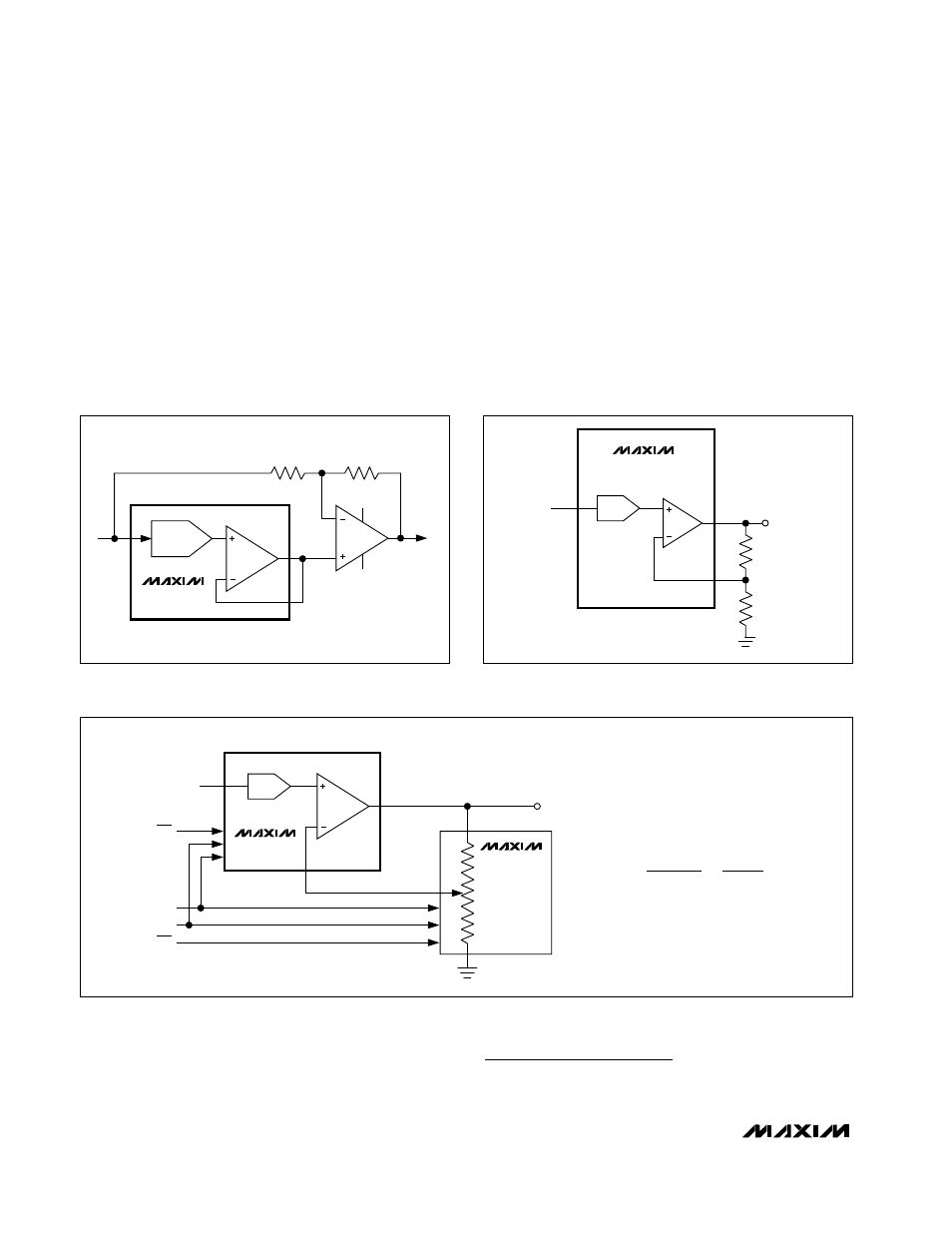
Figure 8. Bipolar Output Circuit
Figure 9. Separate Force-Sense Outputs Create Unity and
Greater-than-Unity DAC Gains Using the Same Reference
REFIN
MAX5530
OUT
V
OUT
FB
V+
10kΩ
10kΩ
V-
DAC
REFIN
V
OUT
OUT
MAX5530
FB
R2
R1
DAC
Figure 10. Software-Configurable Output Gain
H
L
FB
W
N
DAC
IS THE NUMERIC VALUE OF THE DAC INPUT CODE.
N
POT
IS THE NUMERIC VALUE OF THE POT INPUT CODE.
REFIN
MAX5530
MAX5401
SOT-POT
100kΩ
VOUT
5PPM/°C
RATIOMETRIC
TEMPCO
1.8V ≤ V
DD
≤ 5.5V
V
OUT
V
OUT
=
V
REFIN
× N
DAC
4096
(
1 +
255 - N
POT
)
255
SCLK
DIN
CS2
CS1
DAC
Chip Information
TRANSISTOR COUNT: 10,688
PROCESS: BiCMOS