Applications information – Rainbow Electronics MAX5531 User Manual
Page 16
MAX5530/MAX5531
Ultra-Low-Power, 12-Bit,
Voltage-Output DACs
16
______________________________________________________________________________________
Applications Information
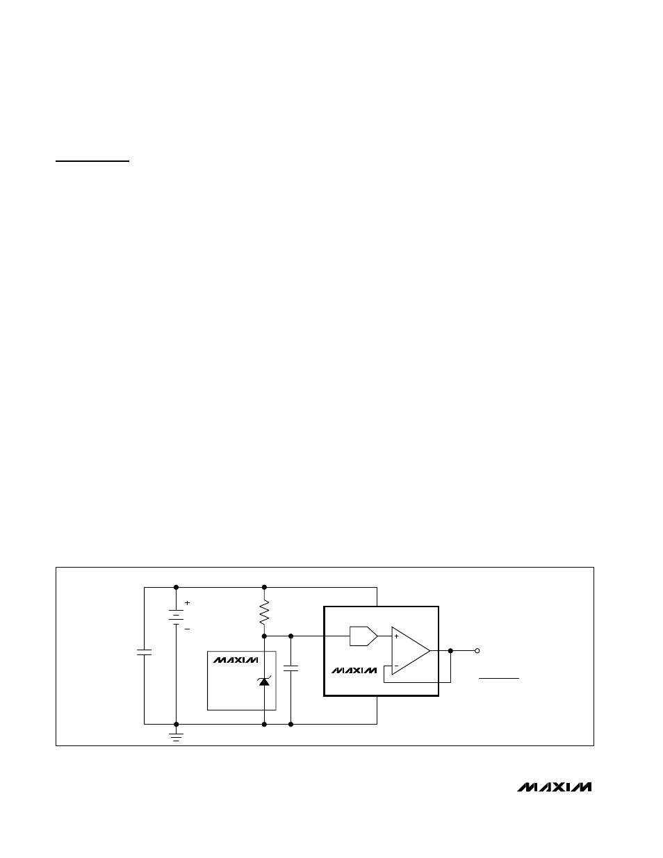
1-Cell and 2-Cell Circuit
See Figure 3 for an illustration of how to power the
MAX5530/MAX5531 with either one lithium-ion battery
or two alkaline batteries. The low current consumption
of the devices makes the MAX5530/MAX5531 ideal for
battery-powered applications.
Programmable Current Source
See the circuit in Figure 4 for an illustration of how to
configure the MAX5530 as a programmable current
source for driving an LED. The MAX5530 drives a stan-
dard NPN transistor to program the current source. The
current source (I
LED
) is defined in the equation in
Figure 4.
Voltage Biasing a Current-Output
Transducer
See the circuit in Figure 5 for an illustration of how to con-
figure the MAX5530 to bias a current output transducer.
In Figure 5, the output voltage of the MAX5530 is a func-
tion of the voltage drop across the transducer added to
the voltage drop across the feedback resistor R.
Self-Biased Two-Electrode
Potentiostat Application
See the circuit in Figure 6 for an illustration of how to
use the MAX5531 to bias a two-electrode potentiostat
on the input of an ADC.
Unipolar Output
Figure 7 shows the MAX5530 in a unipolar output con-
figuration with unity gain. Table 4 lists the unipolar out-
put codes.
Bipolar Output
The MAX5530 output can be configured for bipolar
operation, as shown in Figure 8. The output voltage is
given by the following equation:
V
OUT
= V
REF
x [(N
A
- 2048) / 2048]
where N
A
represents the numeric value of the DAC’s
binary input code. Table 5 shows digital codes (offset
binary) and the corresponding output voltage for the
circuit in Figure 4.
Configurable Output Gain
The MAX5530/MAX5531 have a force-sense output,
which provides a connection directly to the inverting ter-
minal of the output op amp, yielding the most flexibility.
The advantage of the force-sense output is that specific
gains can be set externally for a given application. The
gain error for the MAX5530/MAX5531 is specified in a
unity-gain configuration (op-amp output and inverting ter-
minals connected), and additional gain error results from
external resistor tolerances. Another advantage of the
force-sense DAC is that it allows many useful circuits to
be created with only a few simple external components.
An example of a custom fixed gain using the force-sense
output of the MAX5530/MAX5531 is shown in Figure 9. In
this example, R1 and R2 set the gain for V
OUT
.
V
OUT
=[(V
REFIN
x N
A
) / 4096] x [1 + (R2 / R1)]
where N
A
represents the numeric value of the DAC
input code.
REFIN
MAX5530
MAX6006
(1µA, 1.25V
SHUNT
REFERENCE)
GND
+1.25V
0.01µF
536kΩ
V
DD
DAC
VOUT
N
DAC
IS THE NUMERIC VALUE
OF THE DAC INPUT CODE.
V
OUT
(0.30mV / LSB)
1.8V ≤ V
ALKALINE
≤ 3.3V
2.2V ≤ V
LITHIUM
≤ 3.3V
V
OUT
=
V
REFIN
× N
DAC
4096
0.1µF
Figure 3. Portable Application Using Two Alkaline Cells or One Lithium Coin Cell