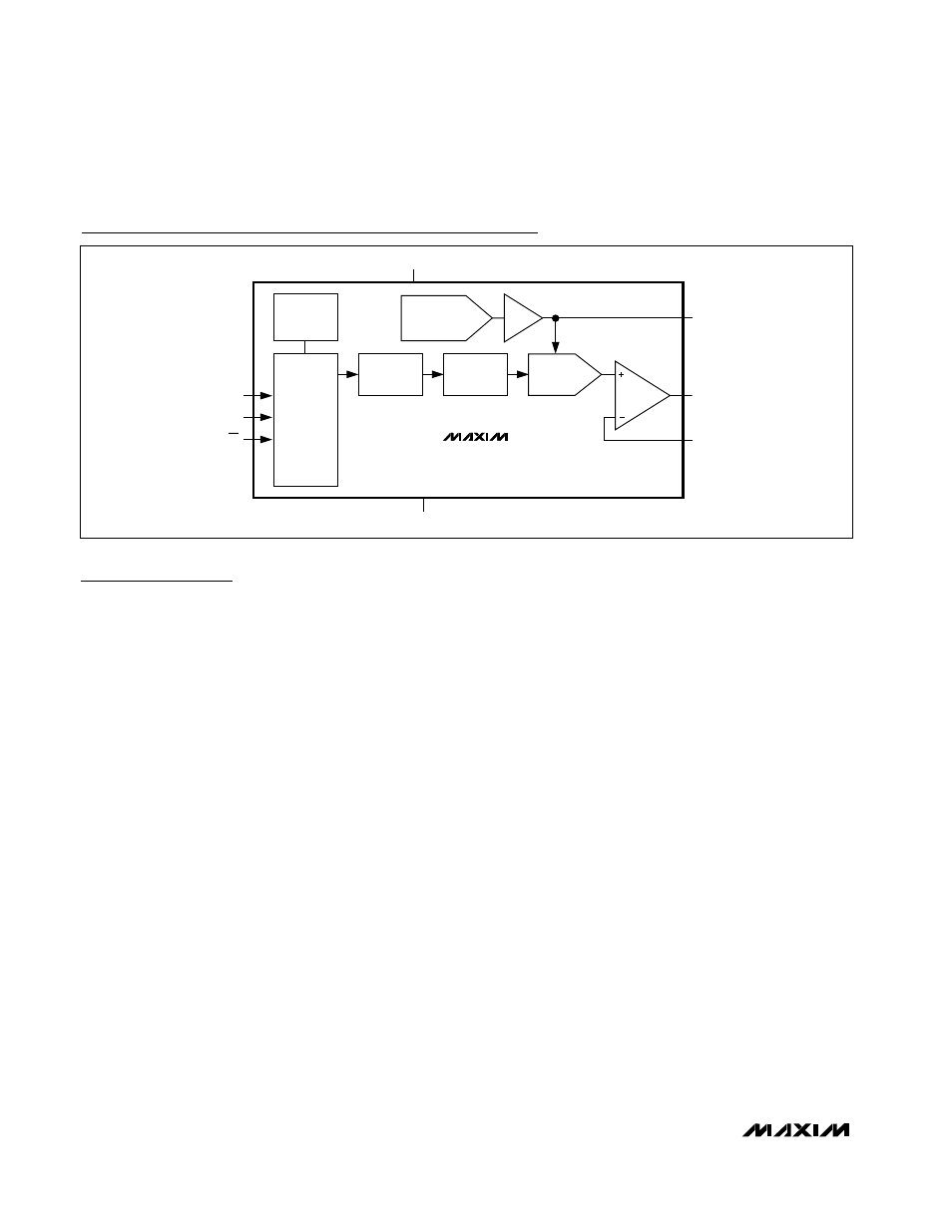
Detailed description, Max5531 functional diagram – Rainbow Electronics MAX5531 User Manual
Page 12
MAX5530/MAX5531
Ultra-Low-Power, 12-Bit,
Voltage-Output DACs
12
______________________________________________________________________________________
Detailed Description
The MAX5530/MAX5531 single, 12-bit, ultra-low-power,
voltage-output DACs offer Rail-to-Rail buffered voltage
outputs. The DACs operate from a 1.8V to 5.5V supply
and require only 6µA (max) supply current. These
devices feature a shutdown mode that reduces overall
current, including the reference input current, to just
0.18µA. The MAX5531 includes an internal reference
that saves additional board space and can source up
to 8mA, making it functional as a system reference. The
16MHz, 3-wire serial interface is compatible with SPI,
QSPI, and MICROWIRE protocols. When V
DD
is
applied, all DAC outputs are driven to zero scale with
virtually no output glitch. The MAX5530/MAX5531 out-
put buffers are configured in force sense allowing users
to externally set voltage gains on the output (an output
amplifier inverting input is available). These devices
come in a 4mm x 4mm thin QFN package.
Digital Interface
The MAX5530/MAX5531 use a 3-wire serial interface
compatible with SPI, QSPI, and MICROWIRE protocols
(Figures 1 and 2).
The MAX5530/MAX5531 include a single, 16-bit, input
shift register. Data loads into the shift register through
the serial interface. CS must remain low until all 16 bits
are clocked in. Data loads MSB first, D11–D0. The 16
bits consist of 4 control bits (C3–C0) and 12 data bits
(D11–D0) (see Table 1). The control bits C3–C0 control
the MAX5530/MAX5531, as outlined in Table 2.
Each DAC channel includes two registers: an input reg-
ister and a DAC register. The input register holds input
data. The DAC register contains the data updated to
the DAC output.
The double-buffered register configuration allows any
of the following:
• Loading the input registers without updating the DAC
registers
• Updating the DAC registers from the input registers
• Updating all the input and DAC registers simultaneously
12-BIT DAC
2-BIT
PROGRAMMABLE
REFERENCE
DAC
REGISTER
OUT
REF
BUF
GND
MAX5531
REFOUT
INPUT
REGISTER
POWER-
DOWN
CONTROL
CONTROL
LOGIC
AND
SHIFT
REGISTER
FB
SCLK
V
DD
DIN
CS
MAX5531 Functional Diagram