Pin description max5530 functional diagram – Rainbow Electronics MAX5531 User Manual
Page 11
MAX5530/MAX5531
Ultra-Low-Power, 12-Bit,
Voltage-Output DACs
______________________________________________________________________________________
11
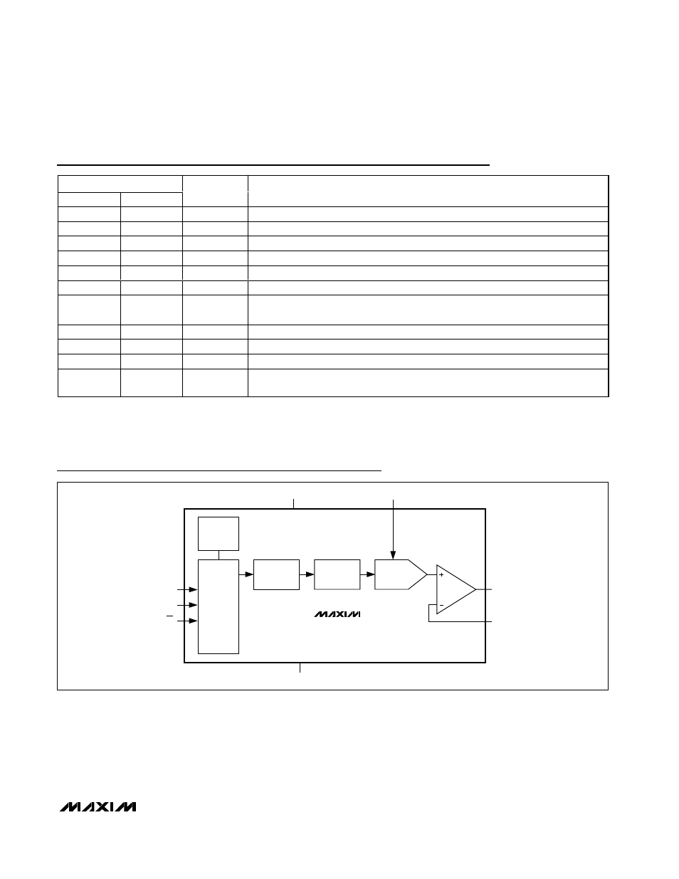
12-BIT DAC
DAC
REGISTER
OUT
REFIN
GND
MAX5530
INPUT
REGISTER
POWER-
DOWN
CONTROL
CONTROL
LOGIC
AND
SHIFT
REGISTER
FB
SCLK
V
DD
DIN
CS
Pin Description
MAX5530 Functional Diagram
PIN
MAX5530
MAX5531
NAME
FUNCTION
1
1
CS
Active-Low Digital-Input Chip Select
2
2
SCLK
Serial-Interface Clock
3
3
DIN
Serial-Interface Data Input
4
—
REFIN
Reference Input
—
4
REFOUT
Reference Output
5, 6, 7, 11
5, 6, 7, 11
N.C.
No Connection. Leave N.C. inputs unconnected (floating) or connected to GND.
8
8
V
DD
Power Input. Connect V
DD
to a 1.8V to 5.5V power supply. Bypass V
DD
to GND with
a 0.1µF capacitor.
9
9
GND
Ground
10
10
OUT
Analog Voltage Output
12
12
FB
Feedback Input
EP
EP
Exposed
Paddle
Exposed Paddle. Connect EP to GND.
- MAX5151 (16 pages)
- MAXQ3108 (64 pages)
- MAX5661 (39 pages)
- MAX6691 (7 pages)
- MAX5362 (12 pages)
- ADC10158 (26 pages)
- MAX8922L (14 pages)
- MAX8596Z (8 pages)
- MAX7491 (18 pages)
- MAX15040 (15 pages)
- MAX5177 (16 pages)
- ADC08138 (22 pages)
- MAX5961 (42 pages)
- T89C51RD2 (86 pages)
- MAX16055 (9 pages)
- MAX6659 (17 pages)
- ADC0820 (20 pages)
- MAX6678 (19 pages)
- MAX8884Z (15 pages)
- MAX16915 (9 pages)
- MAX8620 (18 pages)
- MAX5144 (12 pages)
- MAX6670 (8 pages)
- MAX8760 (39 pages)
- W78C32C (14 pages)
- MX7533 (8 pages)
- MAX8727 (13 pages)
- MAX9053 (15 pages)
- W78C54 (16 pages)
- MAX8614B (15 pages)
- W90N740 (219 pages)
- MAX6626 (13 pages)
- ADC10738 (30 pages)
- MAX17000 (31 pages)
- MAX5051 (21 pages)
- MAXQ1004 (18 pages)
- MAX6871 (51 pages)
- MX7847 (12 pages)
- MAX6608 (6 pages)
- MAX17083 (15 pages)
- MAX6641 (17 pages)
- MAX5251 (16 pages)
- MAX6338 (8 pages)
- MAX6690 (16 pages)
- MAX8668 (18 pages)