Pin description – Rainbow Electronics MAX17062 User Manual
Page 6
MAX17062
TFT-LCD Step-Up DC-DC Converter
6
_______________________________________________________________________________________
PIN
NAME
FUNCTION
1 COMP
Compensation Pin for Error Amplifier. Connect a series RC from COMP to ground. See the Loop
Compensation section for component selection guidelines.
2 FB
Feedback Pin. The FB regulation voltage is 1.24V nominal. Connect an external resistive voltage-divider
between the step-up regulator’s output (V
OUT
) and AGND, with the center tap connected to FB. Place the
divider close to the IC and minimize the trace area to reduce noise coupling. Set V
OUT
according to the
Output Voltage Selection section.
3
SHDN Shutdown Control Input. Drive SHDN low to turn off the MAX17062.
4, 5
PGND
Power Ground. Connect pins 4 and 5 directly together.
6, 7
LX
Switch Pin. LX is the drain of the internal MOSFET. Connect the inductor/rectifier diode junction to LX and
minimize the trace area for lower EMI. Connect pins 6 and 7 together.
8
IN
Supply Pin. Bypass IN with a minimum 1μF ceramic capacitor directly to AGND.
9 FREQ
Frequency-Select Input. When FREQ is low, the oscillator frequency is set to 640kHz. When FREQ is high,
the frequency is 1.2MHz. This input has a 6μA pulldown current.
10 SS
Soft-Start Control Pin. Connect a soft-start capacitor (C
SS
) to this pin. Leave open for no soft-start. The soft-
start capacitor is charged with a constant current of 4μA. Full current limit is reached when the voltage of
SS pin is charged to 1.5V, which is the current-limit time, t = 2.4
10
5
C
SS
. The soft-start capacitor is
discharged to ground when
SHDN is low. When SHDN goes high, the soft-start capacitor is charged to 0.4V,
after which soft-start begins.
EP
AGND
Exposed Pad. Connect to AGND.
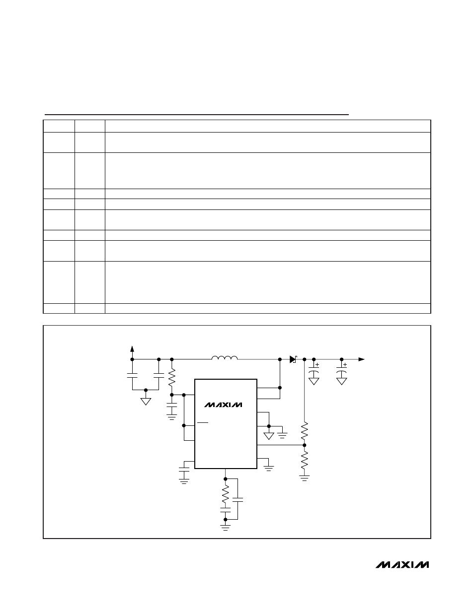
Pin Description
FB
PGND
PGND
AGND
EP
FREQ
IN
COMP
SS
1
4
5
LX
7
LX
6
2
9
3
8
10
V
OUT
+15V/600mA
V
IN
4.5V TO 5.5V
SHDN
MAX17062
C2
4.7
μF
10V
C1
4.7
μF
10V
R1
10
Ω
C3
1
μF
C4
33nF
C5
560pF
C6
OPEN
L1
2.7
μH
D1
R2
47k
Ω
R3
20k
Ω
R4
221k
Ω
C7
10
μF
25V
C8
10
μF
25V
Figure 1. Typical Operating Circuit