Multiple-output power supply for tft-lcd, Pcb layout and grounding – Rainbow Electronics MAX17062 User Manual
Page 11
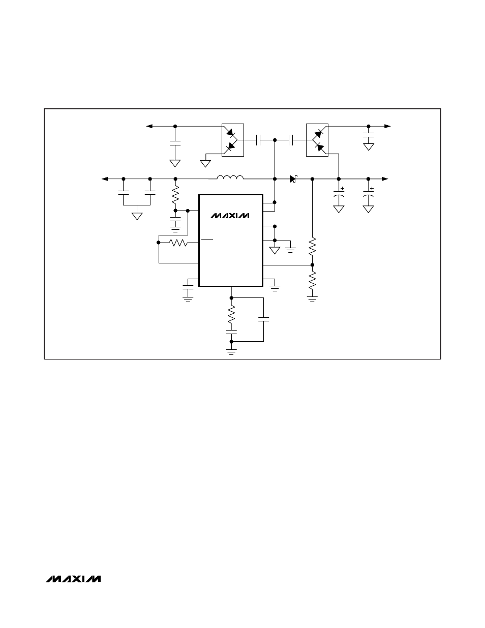
Multiple-Output Power Supply for TFT-LCD
Figure 3 shows a power supply for active-matrix TFT-
LCD flat-panel displays. Output-voltage transient perfor-
mance is a function of the load characteristic. Add or
remove output capacitance (and recalculate compensa-
tion-network component values) as necessary to meet
the required transient performance. Regulation perfor-
mance for secondary outputs (VGON and VGOFF)
depends on the load characteristics of all three outputs.
PCB Layout and Grounding
Careful PCB layout is important for proper operation. Use
the following guidelines for good PCB layout:
1) Minimize the area of high-current loops by placing
the inductor, rectifier diode, and output capacitors
near the input capacitors and near the LX and
PGND pins. The high-current output loop goes from
the positive terminal of the input capacitor to the
inductor, to the IC’s LX pin, out of PGND, and to the
input capacitor’s negative terminal. The high-cur-
rent output loop is from LX switch node to the recti-
fier diode (D1) to the output capacitors, and
reconnecting negative terminals of output capaci-
tors to PGND of the IC. This loop has very high
di/dt, and it is critical to minimize the area of this
loop. Connect these loop components with short,
wide connections. Avoid using vias in the high-cur-
rent paths. If vias are unavoidable, use many vias in
parallel to reduce resistance and inductance.
2) Create a power ground island (PGND) consisting of
the input and output capacitor grounds and PGND
pins. Connect all these together with short, wide
traces or a small ground plane. Maximizing the
width of the power ground traces improves efficien-
cy and reduces output voltage ripple and noise
spikes. Create an analog ground plane (AGND)
consisting of the feedback-divider ground connec-
tion, the COMP and SS capacitor ground connec-
tions, and the device’s exposed backside pad.
Connect the AGND and PGND islands by connect-
ing the PGND pins directly to the exposed backside
pad. Make no other connections between these
separate ground planes.
MAX17062
TFT-LCD Step-Up DC-DC Converter
______________________________________________________________________________________
11
FB
PGND
LX
PGND
FREQ
IN
COMP
SS
1
4
AGND
EP
5
2
9
3
8
10
V
IN
4.5V TO 5.5V
SHDN
MAX17062
U1
C2
4.7
μF
10V
C1
4.7
μF
10V
R1
100k
Ω
R5
10
Ω
C3
1
μF
C4
33nF
C5
560pF
C6
OPEN
L1
2.7
μH
D1
6
LX
7
R2
47k
Ω
R3
20k
Ω
R4
221k
Ω
C11
0.22
μF
C15
0.22
μF
D2
D3
1
3
3
2
2
1
C12
0.1
μF
C14
0.1
μF
V
OUT
+15V/600mA
C7
10
μF
25V
C8
10
μF
25V
VGOFF
-15V
VGON
+29V
Figure 3. Multiple-Output TFT-LCD Power Supply