C timing characteristics – Rainbow Electronics MAX7359 User Manual
Page 3
MAX7359
2-Wire Interfaced Low-EMI
Key Switch Controller/GPO
_______________________________________________________________________________________
3
I
2
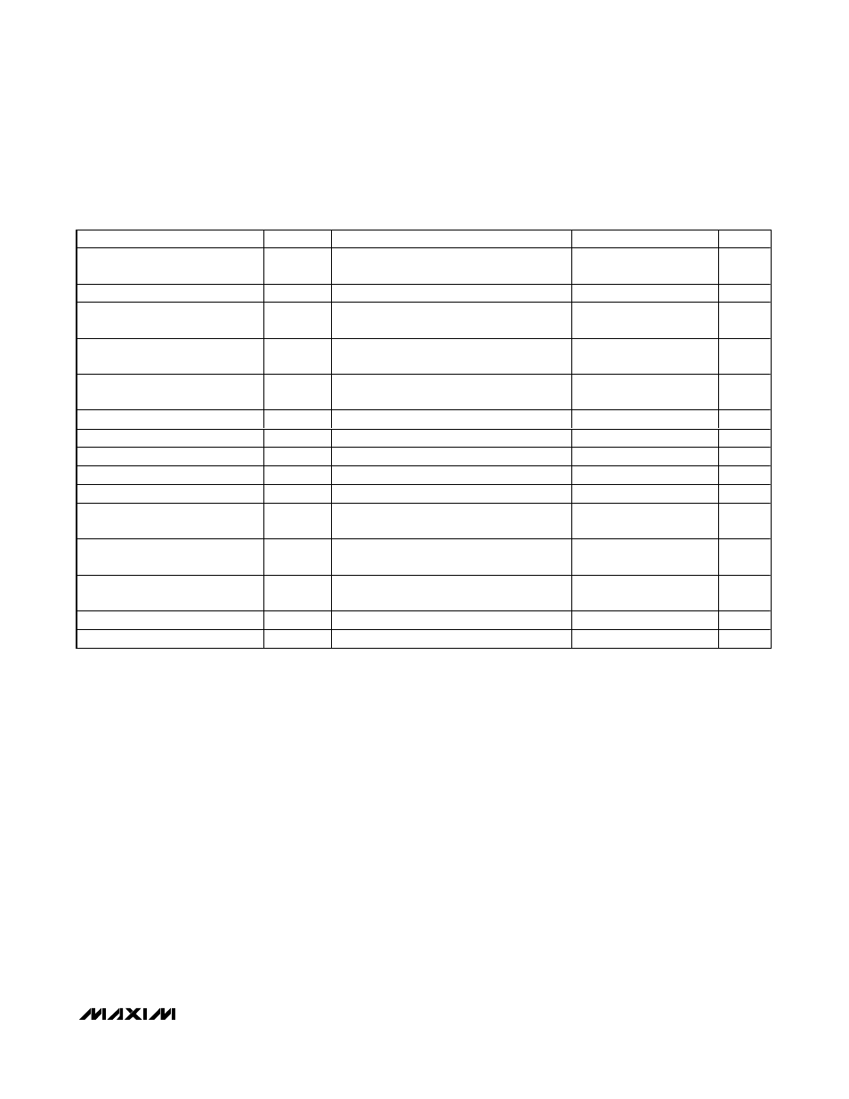
C TIMING CHARACTERISTICS
(V
CC
= 1.62V to 3.6V, T
A
= T
MIN
to T
MAX
, unless otherwise noted. Typical values are at V
CC
= 2.5V, T
A
= +25°C.) (Notes 1, 2) (Figure 2)
PARAMETER
SYMBOL
CONDITIONS
MIN
TYP
MAX
UNITS
Input Capacitance
(SCL, SDA, AD0)
C
IN
(Notes 3, 4)
10
pF
SCL Serial-Clock Frequency
f
SCL
Bus timeout disabled
0
400
kHz
Bus Free Time Between a STOP
and a START Condition
t
BUF
1.3
µs
Hold Time (Repeated) START
Condition
t
HD, STA
0.6
µs
Repeated START Condition
Setup Time
t
SU, STA
0.6
µs
STOP Condition Setup Time
t
SU, STO
0.6
µs
Data Hold Time
t
HD, DAT
(Note 5)
0.9
µs
Data Setup Time
t
SU, DAT
100
ns
SCL Clock Low Period
t
LOW
1.3
µs
SCL Clock High Period
t
HIGH
0.7
µs
Rise Time of Both SDA and SCL
Signals, Receiving
t
R
(Notes 3, 4)
20 +
0.1C
b
300
ns
Fall Time of Both SDA and SCL
Signals, Receiving
t
F
(Notes 3, 4)
20 +
0.1C
b
300
ns
Fall Time of SDA Transmitting
t
F.TX
(Notes 3, 6)
20 +
0.1C
b
250
ns
Pulse Width of Spike Suppressed
t
SP
(Notes 3, 7)
50
ns
C ap aci ti ve Load for E ach Bus Li ne
C
b
(Note 3)
400
pF
Note 1: All parameters are tested at T
A
= +25°C. Specifications over temperature are guaranteed by design.
Note 2: All digital inputs at V
CC
or GND.
Note 3: Guaranteed by design.
Note 4: C
b
= total capacitance of one bus line in pF. t
R
and t
F
measured between 0.8V and 2.1V.
Note 5: A master device must provide a hold time of at least 300ns for the SDA signal (referred to V
IL
of the SCL signal) to bridge
the undefined region of SCL’s falling edge.
Note 6: I
SINK
≤ 6mA. C
b
= total capacitance of one bus line in pF. t
R
and t
F
measured between 0.8V and 2.1V.
Note 7: Input filters on the SDA, SCL, and AD0 inputs suppress noise spikes less than 50ns.