Rainbow Electronics MAX5233 User Manual
Page 2
MAX5232/MAX5233
3V/5V, 10-Bit, Serial Voltage-Output Dual DACs
with Internal Reference
2
_______________________________________________________________________________________
ABSOLUTE MAXIMUM RATINGS
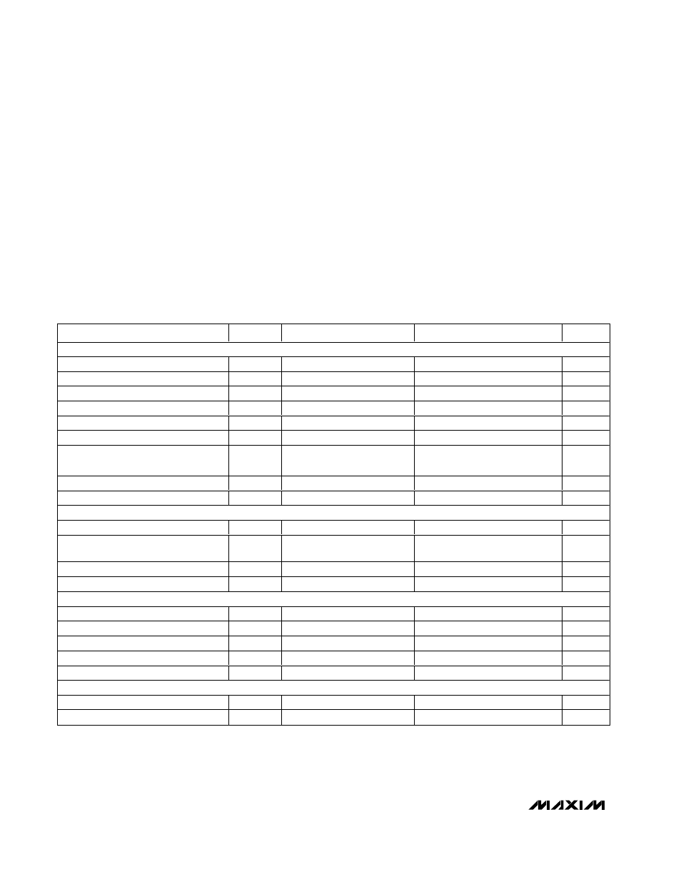
ELECTRICAL CHARACTERISTICS—MAX5233
(V
DD
= +4.5V to +5.5V, OS_ = AGND = DGND = 0, R
L
= 5k
Ω, C
L
= 100pF, T
A
= T
MIN
to T
MAX
, unless otherwise noted. Typical values
are at T
A
= +25°C.)
Stresses beyond those listed under “Absolute Maximum Ratings” may cause permanent damage to the device. These are stress ratings only, and functional
operation of the device at these or any other conditions beyond those indicated in the operational sections of the specifications is not implied. Exposure to
absolute maximum rating conditions for extended periods may affect device reliability.
V
DD
to AGND, DGND ...............................................-0.3V to +6V
AGND to DGND.....................................................-0.3V to +0.3V
Digital Inputs to DGND.............................................-0.3V to +6V
Digital Output (DOUT) to DGND...................-0.3V to V
DD
+ 0.3V
OUT_ to AGND .............................................-0.3V to V
DD
+ 0.3V
OS_ to AGND...................................................-4V to V
DD
+ 0.3V
Maximum Current into Any Pin............................................50mA
Continuous Power Dissipation (T
A
= +70°C)
16-Pin QSOP (derate 8.3mW/°C above +70°C)...........667mW
Operating Temperature Range ...........................-40°C to +85°C
Storage Temperature Range .............................-65°C to +150°C
Lead Temperature (soldering, 10s) .................................+300°C
PARAMETER
SYMBOL
CONDITIONS
MIN
TYP
MAX
UNITS
STATIC PERFORMANCE
Resolution
N
10
Bits
Integral Nonlinearity (Note 1)
INL
±0.5
LSB
Differential Nonlinearity
DNL
±1
LSB
Offset Error (Note 2)
V
OS
±3
mV
Offset-Temperature Coefficient (Note 3)
TCV
OS
8
µV/°C
Full-Scale Voltage
V
FS
Code = 3FF hex, T
A
= +25°C
4.067
4.092
4.117
V
Full-Scale Temperature Coefficient
(Notes 3 and 6)
TCV
FS
10
30
ppm/°C
Power-Supply Rejection
PSR
4.5V
≤ V
DD
≤ 5.5V
30
200
µV
DC Crosstalk (Note 4)
100
µV
REFERENCE
Output-Voltage
V
REF
2.465
V
Output Voltage Temperature Coefficient
(Note 3)
TCV
REF
10
ppm/°C
Reference External Load Regulation
V
OUT
/I
OUT
0
≤ I
OUT
≤ 100µA (sourcing)
0.1
2
µV/µA
Reference Short-Circuit Current
4
mA
DIGITAL INPUTS
Input High Voltage
V
IH
0.7 x V
DD
V
Input Low Voltage
V
IL
0.3 x V
DD
V
Input Hysteresis
V
HYS
200
mV
Input Leakage Current
I
IN
Digital inputs = 0 or V
DD
±1
µA
Input Capacitance
C
IN
8
pF
DIGITAL OUTPUTS
Output High Voltage
V
OH
I
SOURCE
= 2mA
4.25
V
Output Low Voltage
V
OL
I
SINK
= 2mA
0.2
V