Detailed description, Internal reference, Output amplifiers – Rainbow Electronics MAX5233 User Manual
Page 11

Detailed Description
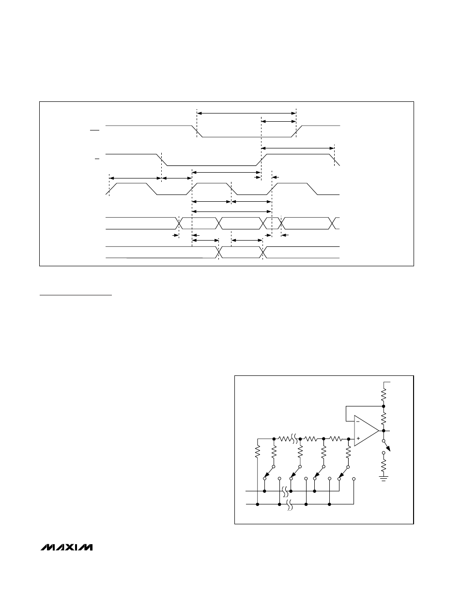
The MAX5232/MAX5233 10-bit, voltage-output DACs
are easily configured with a 3-wire SPI-, QSPI-,
MICROWIRE-compatible serial interface. The devices
include a 16-bit data-in/data-out shift register and have
an input consisting of an input register and a DAC reg-
ister. In addition, these devices employ precision
trimmed internal resistors to produce a gain of
1.6384V/V, maximizing the output voltage swing, and a
programmable-shutdown output impedance of 1k
Ω or
200k
Ω The full-scale output voltage is 4.092V for the
MAX5233 and 2.046V for the MAX5232. These devices
produce a weighted output voltage proportional to the
digital input code with an inverted Rail-to-Rail
®
ladder
network (Figure 3).
Internal Reference
The MAX5230/MAX5231 use an on-board precision
bandgap reference to generate an output voltage of
1.234V (MAX5232) or 2.465V (MAX5233). With a low
temperature coefficient of only 10ppm/°C, REF can
source up to 100µA and is stable for capacitive loads
less than 200pF.
Output Amplifiers
The output amplifiers have internal resistors that pro-
vide for a gain of 1.6384V/V when OS_ is connected to
AGND. The output amplifiers have a typical slew rate of
0.6V/µs and settle to 1/2LSB within 10µs with a load of
5k
Ω in parallel with 100pF. Use the serial interface to
set the shutdown output impedance of the amplifiers to
1k
Ω or 200kΩ.
OS_ can be used to produce an offset voltage at the
output. For instance, to achieve a 1V offset, apply -1V
to OS_ to produce an output range from 1V to (1V +
V
FS
/V
REF
). Note that the DAC’s output range is still lim-
ited by the maximum output voltage specification.
MAX5232/MAX5233
3V/5V, 10-Bit, Serial Voltage-Output Dual DACs
with Internal Reference
______________________________________________________________________________________
11
CS
SCLK
DIN
DOUT
t
CSW
t
CS1
t
CSH
t
CSS
t
CSO
t
D02
t
CH
t
CL
t
CP
t
D01
t
DS
t
DH
t
LDL
LDAC
t
CSLD
Figure 2. Detailed Serial Interface Timing
OUT_
OS_
SHOWN FOR ALL ONES ON DAC
D9
D8
D7
D0
2R
121k
Ω
77.25k
Ω
1k
Ω
2R
2R
2R
2R
R
R
R
REF
AGND
Figure 3. Simplified DAC Circuit Diagram
Rail-to-Rail is a registered trademark of Nippon Motorola, Ltd.
