Applications information, Chip information – Rainbow Electronics MAX5100 User Manual
Page 7
When WR is low, the addressed DAC’s input latch is
transparent. Data is latched when WR is high.
The MAX5100 LDAC feature allows simultaneous
updating of all four DACs. LDAC low latches the data in
the data registers to the DAC registers. If simultaneous
updating is not required, tie LDAC low to keep the DAC
latches transparent. If WR and LDAC are low simultane-
ously, avoid output glitches by ensuring that data is
valid before the two signals go low. When the device
powers up (i.e., V
DD
ramps up), all latches are internal-
ly preset with code 00 hex.
Applications Information
External Reference
The reference source resistance must be considerably
less than the reference input resistance. To keep within
1LSB error in an 8-bit system, R
S
must be less than
R
REF
/ 256. Hence, maintain a value of R
S
<1k
Ω to
ensure 8-bit accuracy. If V
REF
is DC only, bypass REF
to GND with a 0.1µF capacitor. Values greater than this
improve noise rejection.
Power Sequencing
The voltage applied to REF should not exceed V
DD
at
any time. If proper power sequencing is not possible,
connect an external Schottky diode between REF and
V
DD
to ensure compliance with the absolute maximum
ratings.
Power-Supply Bypassing and
Ground Management
Digital or AC transient signals on GND can create noise
at the analog output. Return GND to the highest-quality
ground available. Bypass V
DD
with a 0.1µF capacitor,
located as close to V
DD
and GND as possible.
Careful PC board ground layout minimizes crosstalk
between the DAC outputs and digital inputs.
Chip Information
TRANSISTOR COUNT: 6848
MAX5100
+2.7V to +5.5V, Low-Power, Quad, Parallel
8-Bit DAC with Rail-to-Rail Voltage Outputs
_______________________________________________________________________________________
7
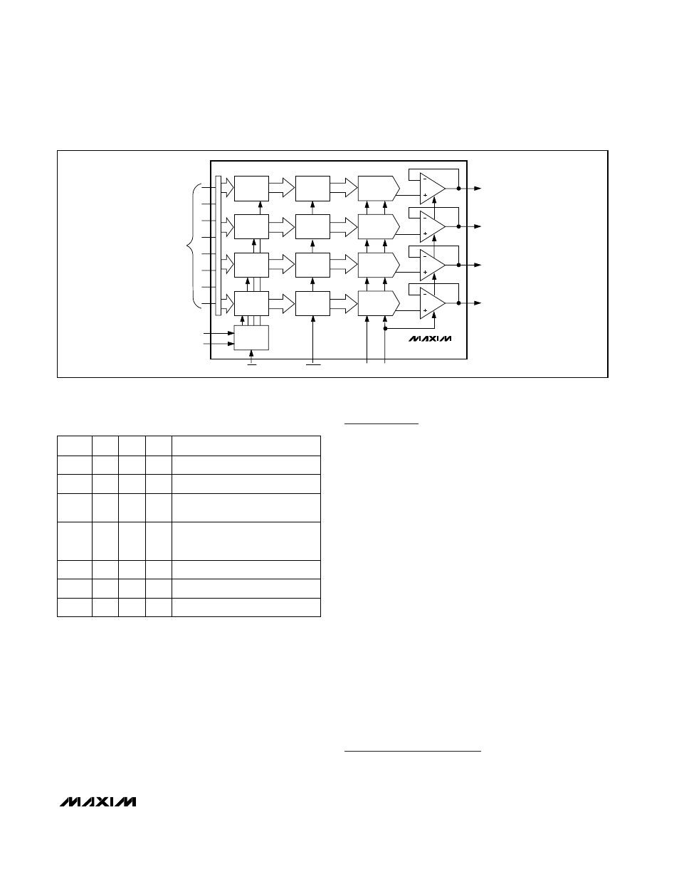
OUTC
OUTD
MAX5100
DAC C
DAC D
INPUT
LATCH C
DAC C
LATCH
INPUT
LATCH D
DAC D
LATCH
CONTROL
LOGIC
SHDN
REF
A1
AO
D0–D7
WR
LDAC
OUTA
OUTB
DAC A
DAC B
INPUT
LATCH A
DAC A
LATCH
INPUT
LATCH B
DAC B
LATCH
Figure 2. Functional Diagram
H = High state, L = Low state, X = Don’t care
Table 1. MAX5100 Address Table (Partial)
A0
X
L
X
L
H
L
H
A1
X
L
X
L
H
H
L
WR
LATCH STATE
H
H
Input and DAC data latched
H
L
DAC A input latch transparent
LDAC
L
H
All 4 DACs’ DAC latches
transparent
L
L
DAC A input registers transpar-
ent and all 4 DACs’ DAC
latches transparent
H
L
DAC D input latch transparent
H
L
DAC C input latch transparent
H
L
DAC B input latch transparent