Rainbow Electronics MAX5100 User Manual
Page 2
MAX5100
+2.7V to +5.5V, Low-Power, Quad, Parallel
8-Bit DAC with Rail-to-Rail Voltage Outputs
2
_______________________________________________________________________________________
ABSOLUTE MAXIMUM RATINGS
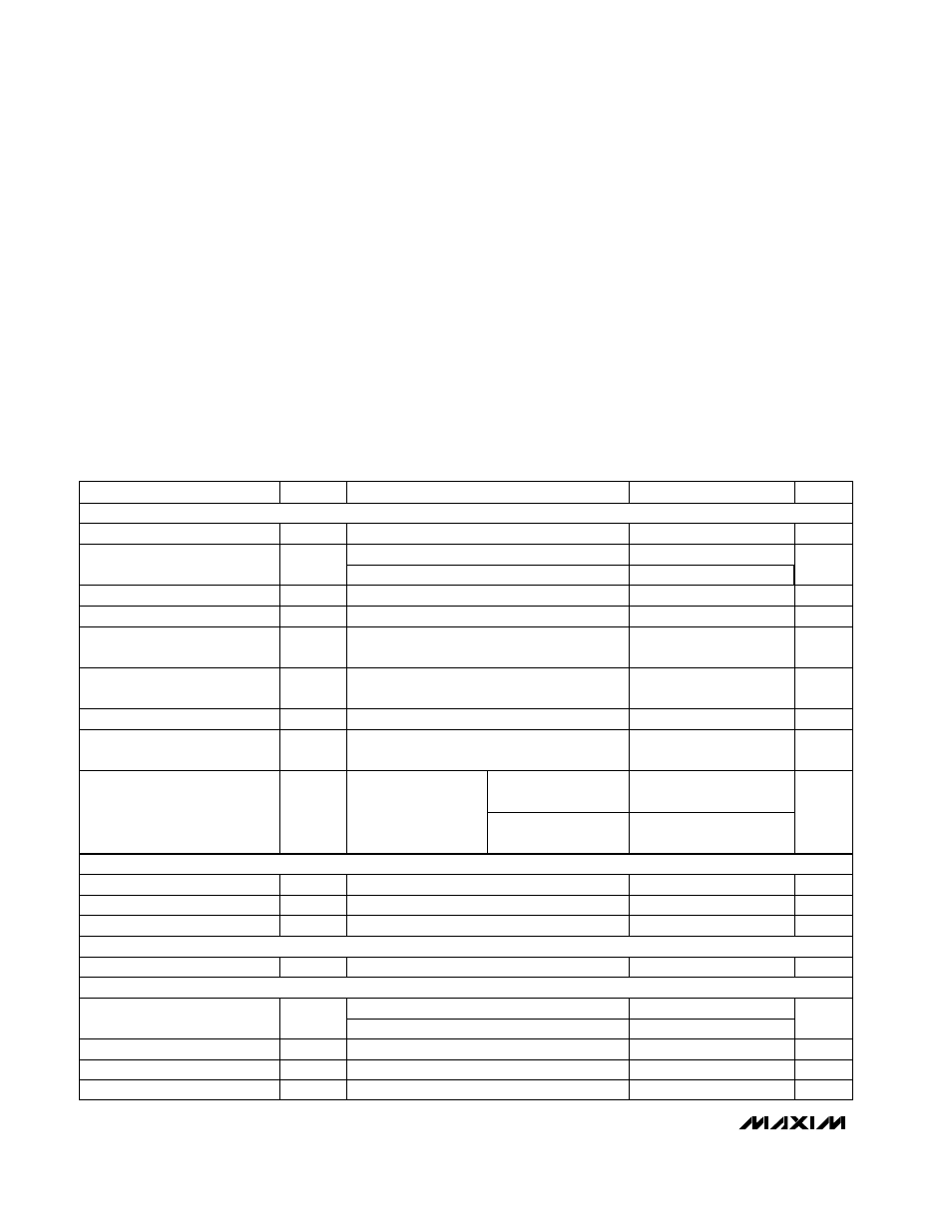
ELECTRICAL CHARACTERISTICS
(V
DD
= V
REF
= +2.7V to +5.5V, R
L
= 10k
Ω, C
L
= 100pF, T
A
= T
MIN
to T
MAX
, unless otherwise noted. Typical values are at V
DD
= V
REF
= +3V and T
A
= +25°C.)
Stresses beyond those listed under “Absolute Maximum Ratings” may cause permanent damage to the device. These are stress ratings only, and functional
operation of the device at these or any other conditions beyond those indicated in the operational sections of the specifications is not implied. Exposure to
absolute maximum rating conditions for extended periods may affect device reliability.
V
DD
to GND ..............................................................-0.3V to +6V
D_, A_, WR, SHDN, LDAC to GND...........................-0.3V to +6V
REF to GND ................................................-0.3V to (V
DD
+ 0.3V)
OUT_ to GND ...........................................................-0.3V to V
DD
Maximum Current into Any Pin .........................................±50mA
Continuous Power Dissipation (T
A
= +70°C)
20-Pin TSSOP (derate 7.0mW/°C above +70°C) .......559mW
Operating Temperature Range
MAX5100_EUP ..............................................-40°C to +85°C
Maximum Junction Temperature .....................................+150°C
Storage Temperature Range .............................-65°C to +150°C
Lead Temperature (soldering, 10sec) .............................+300°C
V
DD
= 4.5V to 5.5V,
V
REF
= 4.096V
V
DD
= 2.7V to 3.6V,
V
REF
= 2.5V
V
IN
= V
DD
or GND
MAX5100A
V
DD
= 3.6V to 5.5V
V
DD
= 2.7V to 3.6V
R
L
=
∞
Code = F0 hex
Code = F0 hex
Code = 00 hex
MAX5100B
Guaranteed monotonic
Code = 00 hex
Code = 00 hex, V
DD
= 2.7V to 5.5V
CONDITIONS
µA
±1.0
I
IN
Input Current
V
0.8
V
IL
Input Low Voltage
3
V
2
V
IH
Input High Voltage
V
0
V
REF
Output Voltage Range
pF
15
Input Capacitance
k
Ω
320
460
600
Input Resistance
V
0
V
DD
Input Voltage Range
1
LSB
±1
INL
Integral Nonlinearity (Note 1)
Bits
8
Resolution
LSB
1
Power-Supply Rejection
LSB/°C
±0.001
Gain-Error Temperature
Coefficient
%
±1
Gain Error (Note 2)
µV/°C
±10
Zero-Code Temperature
Coefficient
±2
LSB
±1
DNL
Differential Nonlinearity (Note 1)
mV
±20
ZCE
Zero-Code Error
mV
10
Zero-Code-Error Supply
Rejection
UNITS
MIN
TYP
MAX
SYMBOL
PARAMETER
pF
10
C
IN
Input Capacitance
Code = FF hex
STATIC ACCURACY
REFERENCE INPUT
DAC OUTPUTS
DIGITAL INPUTS