Rainbow Electronics MAX16054 User Manual
Page 5

Undervoltage Lockout
The undervoltage-lockout circuitry ensures that the out-
puts are at the correct state on power-up. While V
CC
is
less than the 2.1V (typ) undervoltage threshold and
greater than 1.0V, OUT remains low and transitions at
IN are ignored.
Robust Switch Input
The switch input (IN) has overvoltage clamping diodes to
protect against damaging fault conditions. Switch input
voltages can safely swing ±25V to ground. Proprietary
ESD-protection structures protect against high ESD
encountered in harsh industrial environments, membrane
keypads, and portable applications. They are designed
to withstand ±15kV per the IEC 61000-4-2 Air-Gap
Discharge test and ±8kV per the IEC 61000-4-2 Contact-
Discharge test.
Since there is a 63kΩ (typ) pullup resistor connected to
IN, driving the input to -25V draws approximately 0.5mA
from the V
CC
supply. Driving the input to +25V causes
approximately 0.32mA of current to flow back into the
V
CC
supply. If the total system V
CC
supply current is
less than the current flowing back into the V
CC
supply,
V
CC
rises above normal levels. In some low-current sys-
tems, a zener diode on V
CC
may be required.
±15kV ESD Protection
ESD-protection structures are incorporated on all pins
to protect against electrostatic discharges encountered
during handling and assembly. The MAX16054 has
extra protection against static electricity to protect
against ESD of ±15kV at the switch input without dam-
age. The ESD structures withstand high ESD in all
states: normal operation, shutdown, and powered
down. A design advantage of the MAX16054 is that it
continues working without latchup after an ESD event,
which eliminates the need to power-cycle the device.
ESD protection can be tested in various ways; this
product is characterized for protection to the following
limits:
1) ±15kV using the Human Body Model.
2) ±8kV using the Contact-Discharge method specified
in IEC 61000-4-2.
3) ±15kV using the IEC 61000-4-2 Air-Gap method.
MAX16054
On/Off Controller with Debounce and
±15kV ESD Protection
_______________________________________________________________________________________
5
V
CC
t
DP
t
DP
t
DP
t
DP
t
DP
t
CO
UVLO
IN
OUTPUT OF D
FLIP-FLOP
(INVERTED
IN AFTER
DEBOUNCE)
OUT
CLEAR
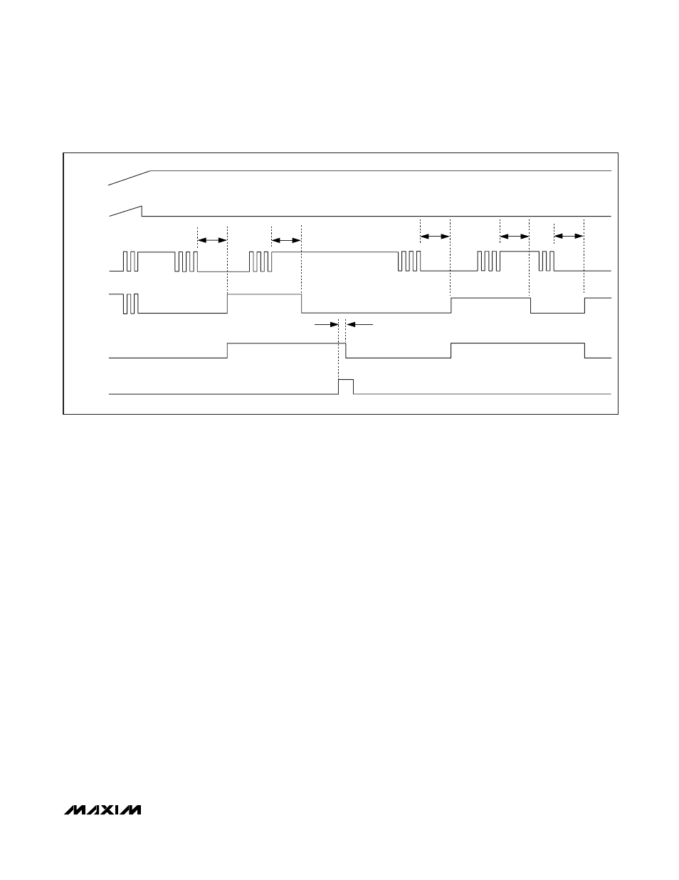
Figure 1. MAX16054 Timing Diagram
