Rainbow Electronics MX7576 User Manual
Page 9

The decoupling capacitors are necessary to provide a
low AC source impedance.
Internal/External Clock
The MX7575/MX7576 can be run with either an exter-
nally applied clock or their internal clock. In either case,
the signal appearing at the clock pin is internally divid-
ed by two to provide an internal clock signal that is rela-
tively insensitive to the input clock duty cycle.
Therefore, a single conversion takes 20 input clock
cycles, which corresponds to 10 internal clock cycles.
Internal Clock
The internal oscillator frequency is set by an external
capacitor, C
CLK
, and an external resistor, R
CLK
, which
are connected as shown in Figure 16a. During a con-
version, a sawtooth waveform is generated on the CLK
pin by charging C
CLK
through R
CLK
and discharging it
through an internal switch. At the end of a conversion,
the internal oscillator is shut down by clamping the CLK
pin to V
DD
through an internal switch. The circuit for the
internal oscillator can easily be overdriven with an
external clock source.
The internal oscillator provides a convenient clock
source for the MX7575. Figure 17 shows typical conver-
sion times versus temperature for the recommended
R
CLK
and C
CLK
combination. Due to process varia-
tions, the oscillation frequency for this R
CLK
/C
CLK
com-
bination may vary by as much as ±50% from the
nominal value shown in Figure 17. Therefore, an exter-
nal clock should be used in the following situations:
1) Applications that require the conversion time to be
within 50% of the minimum conversion time for the
specified accuracy (5µs MX7575/10µs MX7576).
2) Applications in which time-related software con-
straints cannot accommodate conversion-time differ-
ences that may occur from unit to unit or over
temperature for a given device.
External Clock
The CLK input of the MX7575/MX7576 may be driven
directly by a 74HC or 4000B series buffer (e g., 4049),
or by an LS TTL output with a 5.6k
Ω
pull-up resistor. At
the end of a conversion, the device ignores the clock
input and disables its internal clock signal. Therefore,
the external clock may continue to run between conver-
sions without being disabled. The duty cycle of the
external clock may vary from 30% to 70%. As dis-
cussed previously, in order to maintain accuracy, clock
rates significantly lower than the data sheet limits
(4MHz for MX7575 and 2MHz for MX7576) should not
be used.
MX7575/MX7576
CMOS, µP-Compatible, 5µs/10µs, 8-Bit ADCs
_______________________________________________________________________________________
9
54
52
50
46
44
42
100
1k
100k
48
40
MX7575/6 FIG13
INPUT FREQUENCY (Hz)
SNR (dB)
10k
T
A
= +25°C
0
0.5
1.0
2.0
2.5
10
100
10000
1.5
MX7575/6 FIG14
CONVERSION TIME (
µ
s)
RELATIVE ACCURACY (LSB)
1000
A
B
C
A: T
A
= +125°C
B: T
A
= +85°C
C: T
A
= +25°C
1.23V
0.1
µ
F
47
µ
F
+5V
REF
3.3k
+
_
+
ICL8069
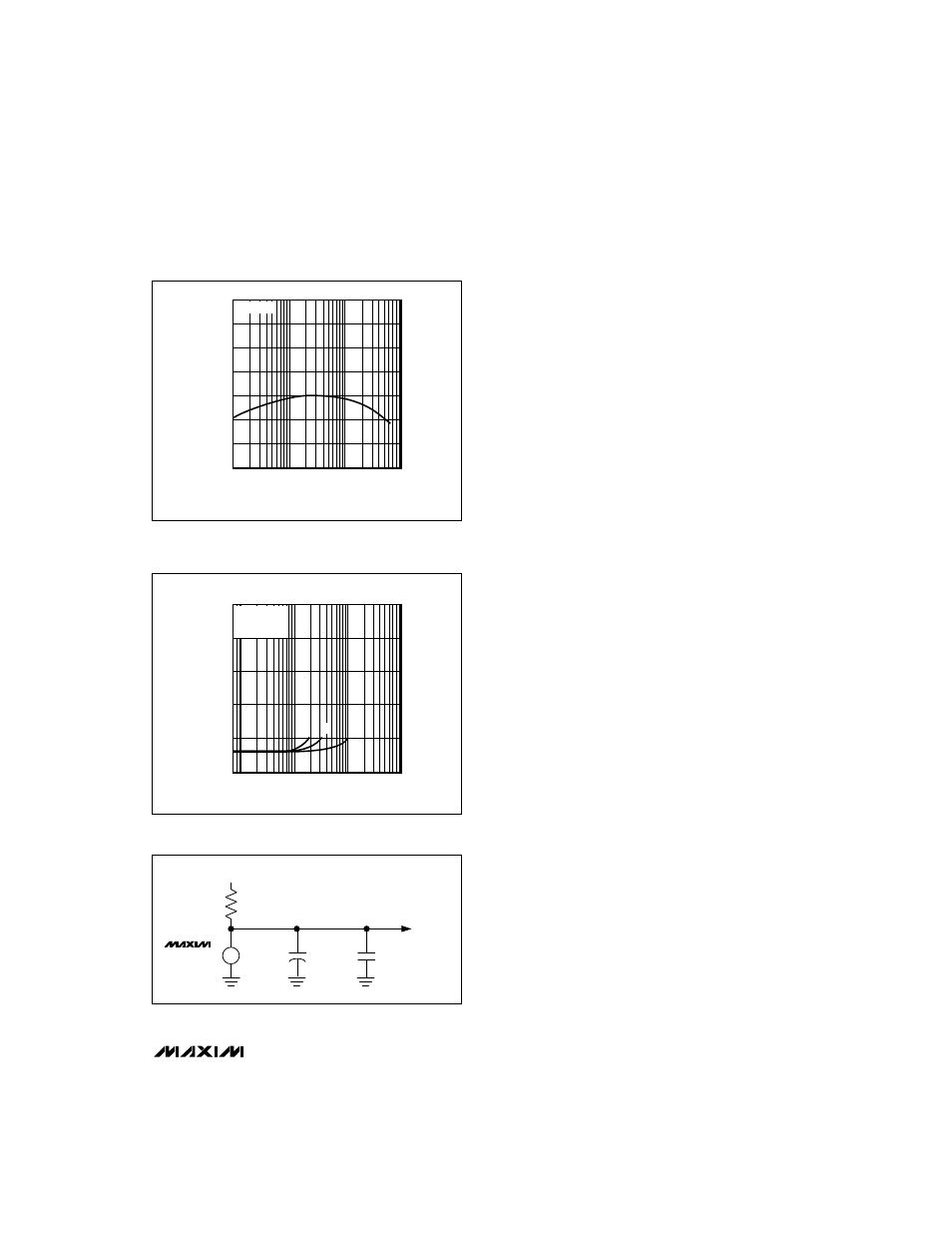
Figure 13. MX7575 SNR vs. Input Frequency
Figure 14. MX7575 Accuracy vs. Conversion Time
Figure 15. External Reference Circuit
