Applications information, Functional diagrams (continued) – Rainbow Electronics MX7576 User Manual
Page 11

__________Applications Information
Noise
To minimize noise coupling, keep both the input signal
lead to AIN and the signal return lead from AGND as
short as possible. If this is not possible, a shielded
cable or a twisted-pair transmission line is recommend-
ed. Additionally, potential differences between the ADC
ground and the signal-source ground should be mini-
mized, since these voltage differences appear as
errors superimposed on the input signal. To minimize
system noise pickup, keep the driving source resis-
tance below 2k
Ω
.
Proper Layout
For PC board layouts, take care to keep digital lines
well separated from any analog lines. Establish a sin-
gle-point, analog ground (separate from the digital sys-
tem ground) near the MX7575/MX7576. This analog
ground point should be connected to the digital system
ground through a single-track connection only. Any
supply or reference bypass capacitors, analog input fil-
ter capacitors, or input signal shielding should be
returned to the analog ground point.
__Functional Diagrams (continued)
MX7575/MX7576
CMOS, µP-Compatible, 5µs/10µs, 8-Bit ADCs
______________________________________________________________________________________
11
17
16
5
15
18
9
+5V
+5V
+5V
47
µ
F
47
µ
F
0.1
µ
F
R6
3.3k
R7
10k
R1
1k
R2
820
Ω
AGND DGND
R3
500
Ω
INPUT VOLTAGE
R5
5k
R4
8.2k
0.1
µ
F
TLC271
+5V
+
D7–D0
DATA OUT
C
L
100pF
2%
R
CLK
REF
AIN
CLK
V
DD
MX7575
ICL8069
1.2V
REFERENCE
111...111
111...110
100...010
100...001
100...000
011...111
011...110
000...001
000...000
OUTPUT
CODE
-FS
2
-1/2LSB
1/2LSB
FS
2
2FS
256
-1LSB
FS = 2V
REF
1LSB =
AIN
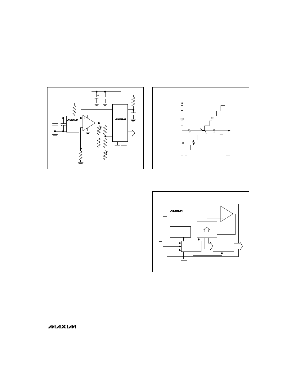
Figure 18a. MX7575 Bipolar Configuration
Figure 18b. Nominal Transfer Characteristic for Bipolar
Operation
DAC
COMP
LATCH AND
THREE-STATE
OUTPUT DRIVERS
SAR
CLOCK
OSCILLATOR
CONTROL
LOGIC
AIN
AGND
REF
CLK
CS
RD
V
DD
BUSY
DGND
MODE
16
18
4
9
6
14
D7
D0
15
17
5
1
2
3
MX7576
..
