Pin description – Rainbow Electronics MX7576 User Manual
Page 4
MX7575/MX7576
CMOS, µP-Compatible, 5µs/10µs, 8-Bit ADCs
4
_______________________________________________________________________________________
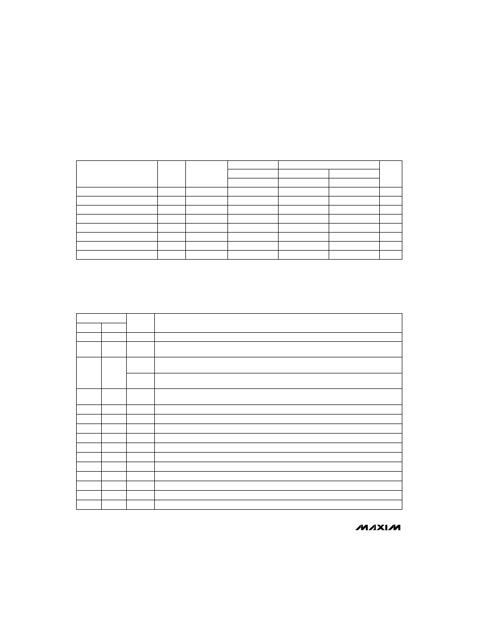
______________________________________________________________Pin Description
DIP/SO
NAME
FUNCTION
1
CS
Chip Select Input.
CS must be low for the device to be selected or to recognize the RD input.
PIN
2
RD
Read Input.
RD must be low to access data. RD is also used to start conversions. See the
Microprocessor Interface
section.
TP
(MX7575)
Test Point. Connect to V
DD
.
7, 8
D6, D5
Three-State Data Outputs, bits 6 and 5
6
D7
Three-State Data Output, bit 7 (MSB)
5
CLK
External Clock Input/Internal Oscillator Pin for frequency setting RC components.
4
BUSY
BUSY Output. BUSY going low indicates the start of a conversion. BUSY going high indicates the
end of a conversion.
9
DGND
Digital Ground
T
A
= +25°C
T
A
= T
MIN
to T
MAX
ALL
J/K/A/B
S/T
PARAMETER
SYMBOL
CONDITIONS
MIN
MAX
MIN
MAX
MIN
MAX
UNITS
CS to RD Setup Time
t
1
0
0
0
ns
RD to BUSY Propagation Time
t
2
100
100
120
ns
Data-Access Time after
RD
t
3
(Note 6)
100
100
120
ns
RD Pulse Width
t
4
100
100
120
ns
CS to RD Hold Time
t
5
0
0
0
ns
Data-Access Time after
BUSY
t
6
(Note 6)
80
80
100
ns
Data-Hold Time
t
7
(Note 7)
10
80
10
80
10
100
ns
BUSY to CS Delay
t
8
0
0
0
ns
TIMING CHARACTERISTICS (Note 5)
(V
DD
= +5V, V
REF
= 1.23V, AGND = DGND = 0V.)
Note 5:
Timing specifications are sample tested at +25°C to ensure compliance. All input control signals are specified with
t
r
= t
f
= 20ns (10% to 90% of +5V) and timed from a voltage level of 1.6V.
Note 6:
t
3
and t
6
are measured with the load circuits of Figure 1 and defined as the time required for an output to cross 0.8V or 2.4V.
Note 7:
t
7
is defined as the time required for the data lines to change 0.5V when loaded with the circuits of Figure 2.
PLCC
2
3
4
8, 9
7
6
5
10
3
MODE
(MX7576)
Mode Input. MODE = low puts the ADC into its asynchronous conversion mode. MODE has to be
tied high for the synchronous conversion mode and the ROM interface mode.
14
D0
Three-State Data Output, bit 0 (LSB)
10–13
D4–D1
Three-State Data Outputs, bits 4–1
15
AGND
Analog Ground
16
12–15
17
18
V
DD
Power-Supply Voltage. +5V nominal.
17
REF
Reference Input. +1.23V nominal.
—
N.C.
No Connect
20
19
1, 11
16
AIN
Analog Input. 0V to 2V
REF
input range.
18