Rainbow Electronics MX7576 User Manual
Page 7

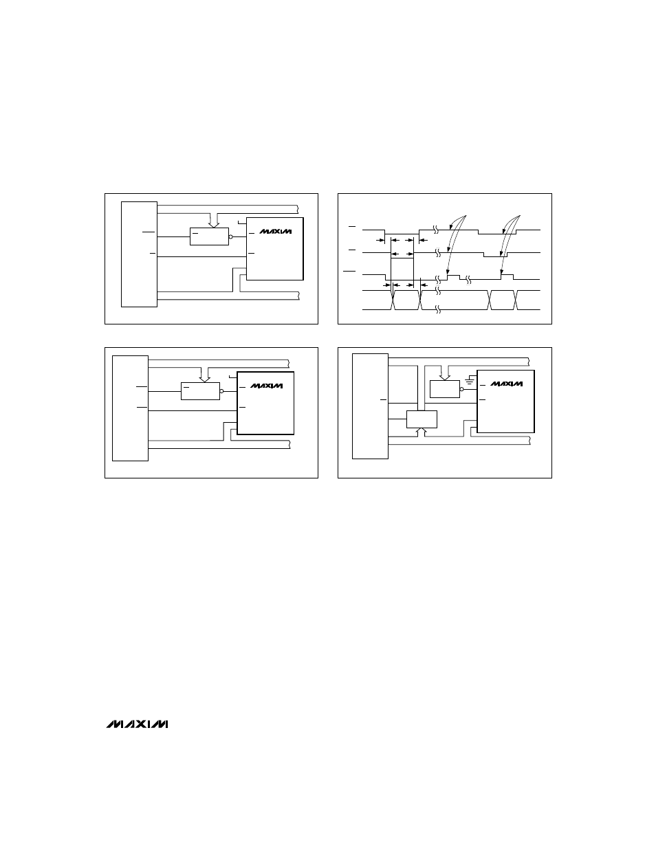
the µP, in that data can be accessed independently of
the clock. The output latches are normally updated on
the rising edge of
BUSY. But if CS and RD are low
when
BUSY goes high, the data latches are not updat-
ed until one of these inputs returns high. Additionally,
the MX7576 stops converting and
BUSY stays high until
RD or CS goes high. This mode of operation allows a
simple interface to the µP.
Processor Interface for Signal Acquisition (MX7575)
In many applications, it is necessary to sample the
input signal at exactly equal intervals to minimize errors
due to sampling uncertainty or jitter. In order to achieve
this objective with the previously discussed interfaces,
the user must match software delays or count the num-
ber of elapsed clock cycles. This becomes difficult in
interrupt-driven systems where the uncertainty in inter-
rupt servicing delays is another complicating factor.
The solution is to use a real-time clock to control the
start of a conversion. This should be synchronous with
the CLK input to the ADC (both should be derived from
the same source), because the sampling instants occur
three clock cycles after
CS and RD go low. Therefore,
the sampling instants occur at exactly equal intervals if
the conversions are started at equal intervals. In this
scheme, the output data is fed into a FIFO latch, which
allows the µP to access data at its own rate. This guar-
antees that data is not read from the ADC in the middle
of a conversion. If data is read from the ADC during a
conversion, the conversion in progress may be dis-
turbed, but the accessed data that belonged to the pre-
vious conversion will be correct.
The track/hold starts holding the input on the third
falling edge of the clock after
CS and RD go low. If CS
and
RD go low within 20ns of a falling clock edge, the
ADC may or may not consider this falling edge as the
first of the three edges that determine the sampling
instant. Therefore, the
CS and RD should not be
allowed to go low within this period when sampling
accuracy is required.
MX7575/MX7576
CMOS, µP-Compatible, 5µs/10µs, 8-Bit ADCs
_______________________________________________________________________________________
7
Figure 7. MX7575/MX7576 to Z-80 ROM Interface
ADDRESS
DECODE
ADDRESS BUS
+5V
DATA BUS
Z-80
MREQ
RD
RD
CS
EN
TP/MODE
D7
D0
DB7
DB0
MX7575*
MX7576
* SOME CIRCUITRY OMITTED FOR CLARITY
Figure 8. MX7575/MX7576 to TMS32010 ROM Interface
ADDRESS
DECODE
ADDRESS BUS
+5V
DATA BUS
PA2
PA0
MEN
DEN
RD
CS
EN
TP/MODE
D7
D0
DB7
DB0
MX7575*
MX7576
TMS32010
* SOME CIRCUITRY OMITTED FOR CLARITY
Figure 9. MX7576 Asynchronous Conversion Mode Timing
Diagram
CS
RD
BUSY
DATA
HIGH-
IMPEDANCE
BUS
HIGH-
IMPEDANCE
BUS
VALID
DATA
t
1
t
5
t
4
t
3
t
7
HIGH-IMPEDANCE BUS
VALID
DATA
UPDATE
LATCH
DEFER
UPDATING
ADDRESS
ENCODE
ADDRESS BUS
DATA BUS
ADDRESS
LATCH
8085A
A0–A15
RD
RD
CS
MODE
D0–D7
ALE
AD0–AD7
MX7576*
* SOME CIRCUITRY OMITTED FOR CLARITY
Figure 10. MX7576 to 8085A Asynchronous Conversion Mode
Interface
