Rainbow Electronics MAX4889C User Manual
Page 2
MAX4889B/MAX4889C
2.5/5.0Gbps PCIe Passive Switches
2
_______________________________________________________________________________________
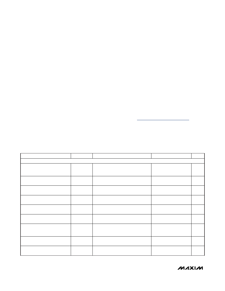
ABSOLUTE MAXIMUM RATINGS
ELECTRICAL CHARACTERISTICS
(V
CC
= +3.3V ±10%, T
A
=T
MIN
to T
MAX,
unless otherwise noted. Typical values are at V
CC
= +3.3V, T
A
= +25°C, unless otherwise
noted.) (Note 3)
Stresses beyond those listed under “Absolute Maximum Ratings” may cause permanent damage to the device. These are stress ratings only, and functional
operation of the device at these or any other conditions beyond those indicated in the operational sections of the specifications is not implied. Exposure to
absolute maximum rating conditions for extended periods may affect device reliability.
(All voltages referenced to GND, unless otherwise noted.)
V
CC
...........................................................................-0.3V to +4V
SEL, _IN_, _OUTA_, _OUTB_ (Note 1) .......-0.3V to (V
CC
+ 0.3V)
Continuous Current (AIN_ to AOUTA_/AOUTB_, BIN_ to
BOUTA_/BOUTB_, CIN_ to COUTA_/COUTB_, DIN_ to
DOUTA_/DOUTB_)........................................................±70mA
Peak Current (AIN_ to AOUTA_/AOUTB_, BIN_ to
BOUTA_/BOUTB_, CIN_ to COUTA_/COUTB_, DIN_ to
DOUTA_/DOUTB_)
(pulsed at 1ms, 10% duty cycle)..............................±70mA
Continuous Current (SEL).................................................±10mA
Peak Current (SEL)
(pulsed at 1ms, 10% duty cycle)..................................±10mA
Continuous Power Dissipation (T
A
= +70°C) for multilayer board:
42-Pin TQFN (derate 35.7mW/°C above +70°C) .......2857mW
Operating Temperature Range ...........................-40°C to +85°C
Junction Temperature ......................................................+150°C
Storage Temperature Range .............................-65°C to +150°C
Package Junction-to-Ambient Thermal Resistance
(
θ
JA
) (Note 2) ............................................................28.0°C/W
Package Junction-to-Case Thermal Resistance
(
θ
JC
) (Note 2) ..............................................................2.0°C/W
Lead Temperature (soldering, 10s) .................................+300°C
PARAMETER
SYMBOL
CONDITIONS
MIN
TYP
MAX
UNITS
DC PERFORMANCE
Analog Signal Range
_IN_,
_OUTA_,
_OUTB_
-0.3
V
CC
-
1.8
V
On-Resistance
R
ON
V
CC
= +3.0V, I
_IN_
= 15mA, V
_OUTA_
,
V
_OUTB_
= 0V, 1.2V
6.4
8.4
Ω
On-Resistance Match Between
Pairs of Same Channel
ΔR
ON
V
CC
= +3.0V, I
_IN_
= 15mA, V
_OUTA_
,
V
_OUTB_
= 0V (Notes 4, 5)
0.1
0.5
Ω
On-Resistance Match Between
Channels
ΔR
ON
V
CC
= +3.0V, I
_IN_
= 15mA, V
_OUTA_
,
V
_OUTB_
= 0V (Notes 4, 5)
0.2
Ω
On-Resistance Flatness
R
FLAT (ON)
V
CC
= +3.0V, I
_IN_
= 15mA, V
_OUTA_
,
V
_OUTB_
= 0V, 1.2V (Notes 5, 6)
0.3
Ω
_OUTA_ or _OUTB_ Off-Leakage
Current
I
_ OU TA _ ( OF F)
,
I
_ OU TB _ ( OF F)
V
CC
= +3.6V , V
_IN_
= 0V, 1.2V, V
_OUTA_
or V
_OUTB_
= 1.2V, 0V (MAX4889B)
-1
+1
µA
_IN_ On-Leakage Current
I
_IN_ (ON)
V
CC
= +3.6V , V
_IN_
= 0V, 1.2V, V
_OUTA_
or V
_OUTB_
= V
_IN_
or unconnected
(MAX4889B)
-1
+1
µA
Output Short-Circuit Current
All other ports are unconnected
(MAX4889C)
5
15
µA
Output Open-Circuit Voltage
All other ports are unconnected
(MAX4889C)
0.2
0.6
0.9
V
Note 1: Signals on SEL, _IN_, _OUTA_, _OUTB_ exceeding V
CC
or GND are clamped by internal diodes. Limit forward-diode current
to maximum current rating.
Note 2: Package thermal resistances were obtained using the method described in JEDEC specification JESD51-7, using a 4-layer
board. For detailed information on package thermal considerations, refer to
www.maxim-ic.com/thermal-tutorial
.