Rainbow Electronics MAX5074 User Manual
Page 9
Power Topology
The two-switch forward converter topology offers out-
standing robustness against faults and transformer
saturation while affording efficient use of the integrated
0.4
Ω power MOSFETs. Voltage-mode control with
feed-forward compensation allows the rejection of
input supply disturbances within a single cycle similar
to that of current-mode controlled topologies.
The two-switch power topology recovers energy stored
in both the magnetizing and the parasitic leakage
inductances of the transformer. The Typical Application
Circuit, forward converter (Figure 3) shows the
schematic diagram of a 48V input and 5V, 3A output
isolated power supply. Figure 4 shows the schematic
diagram of a flyback converter using the MAX5074.
Undervoltage Lockout (UVLO)
The UVLO block monitors the input voltage HVIN
through an external resistive divider (R24 and R25)
connected to UVLO (see Figure 3). Use the following
equation to calculate R24 and R25:
where V
UVLOIN
is the desired input voltage lockout
level and V
UVLO
is the undervoltage lockout threshold
(1.25V, typ).
Internal Regulators
As soon as power is provided to HVIN, internal power
supplies power the UVLO detection circuitry. REGOUT is
used to drive the internal power MOSFETs. Bypass
REGOUT with a minimum 2.2µF ceramic capacitor. The
HVIN LDO steps down V
HVIN
to a nominal output voltage
(REGOUT) of 8.75V. A second parallel LDO powers
REGOUT from INBIAS. A tertiary winding connected
through a diode to INBIAS powers up REGOUT once
switching commences. This will bring REGOUT to 10.5V
(typ) and shut off the current flowing from HVIN to
REGOUT. This results in a lower on-chip power dissipa-
tion and higher efficiency.
Soft-Start
Program the MAX5074 soft-start with an external capaci-
tor between CSS and GND. When the device turns on,
the soft-start capacitor (C
CSS
) charges with a constant
current of 33µA, ramping up to 7.3V. During this time,
the feedback pin (OPTO) is clamped to V
CSS
+ 0.6V.
This initially holds the duty cycle lower than the value
the regulator tries to impose, thus preventing voltage
overshoot at the output. When the MAX5074 turns off,
the soft-start capacitor internally discharges to GND.
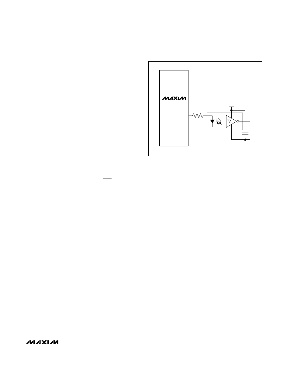
Secondary-Side Synchronization
The MAX5074 provides convenient synchronization for
optional secondary-side synchronous rectifiers. Figure 2
shows the connection diagram with a high-speed opto-
coupler. Choose an optocoupler with a propagation delay
of less than 80ns. The synchronizing pulse is generated
approximately 110ns ahead of the main pulse that drives
the two power MOSFETs.
Voltage-Mode Control and the PWM Ramp
For voltage-mode control, the feed-forward PWM ramp is
generated at RCFF. From RCFF, connect a capacitor to
GND and a resistor to HVIN. The ramp generated is
applied to the noninverting input of the PWM comparator
at RAMP and has a minimum voltage of approximately
2V. The slope of the ramp is determined by the voltage
at HVIN and affects the overall loop gain. The ramp peak
must remain below the dynamic range of RCFF of 5.5V.
Assuming the maximum duty cycle approaches 50% at
a minimum input voltage (PWM UVLO turn-on threshold),
use the following formula to calculate the minimum value
of either the ramp capacitor or resistor:
where f
S
is the switching frequency, V
R(P-P)
is the
peak-to-peak ramp voltage (2V, typ).
R
C
V
f V
RCFF RCFF
UVLOIN
S R P P
≥
−
2
(
)
V
V
R
R
UVLOIN
UVLO
=
×
+
⎛
⎝⎜
⎞
⎠⎟
1
24
25
MAX5074
Power IC with Integrated MOSFETs for Isolated IEEE
802.3af PD and Telecom Power-Supply Applications
_______________________________________________________________________________________
9
PS9715
OR EQUIVALENT
HIGH-SPEED
OPTOCOUPLER
C
5V
R
MAX5074
U1
PPWM
PGND
U2
Figure 2. Secondary-Side Synchronous Rectifier Driver Using a
High-Speed Optocoupler