Rainbow Electronics MAX5074 User Manual
Page 2
MAX5074
Power IC with Integrated MOSFETs for Isolated IEEE
802.3af PD and Telecom Power-Supply Applications
2
_______________________________________________________________________________________
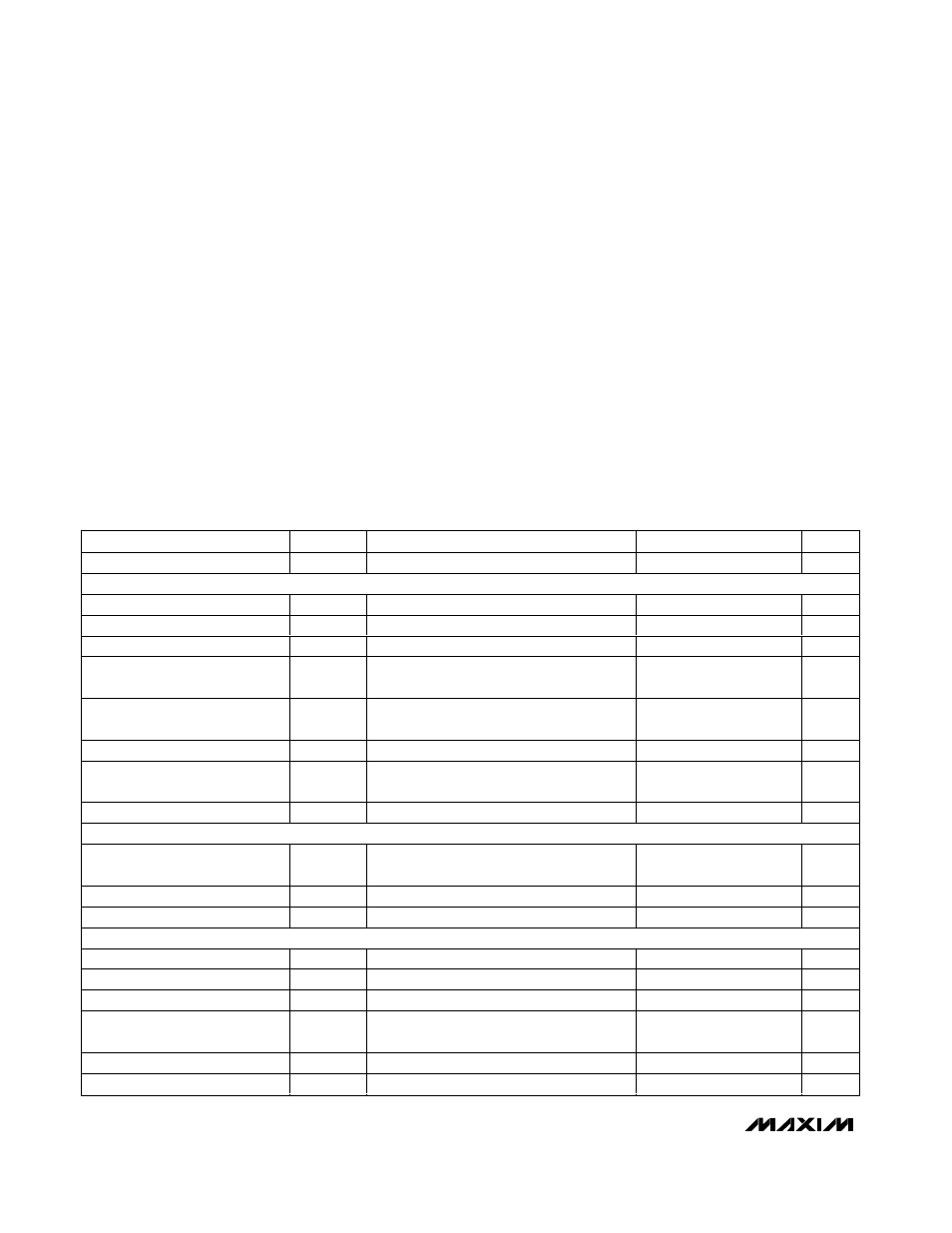
ABSOLUTE MAXIMUM RATINGS
ELECTRICAL CHARACTERISTICS
(V
HVIN
= 12V, C
INBIAS
= 1µF, C
REGOUT
= 2.2µF, R
RTCT
= 25k
Ω, C
RTCT
= 100pF, C
BST
= 0.22µF, V
CSS
= V
CS
= 0V, V
RAMP
= V
UVLO
= 3V,
T
A
= T
J
= -40°C to +125°C, unless otherwise noted. Typical values are at T
A
= +25°C, unless otherwise noted.) (Note 1)
Stresses beyond those listed under “Absolute Maximum Ratings” may cause permanent damage to the device. These are stress ratings only, and functional
operation of the device at these or any other conditions beyond those indicated in the operational sections of the specifications is not implied. Exposure to
absolute maximum rating conditions for extended periods may affect device reliability.
HVIN, INBIAS, DRNH, XFRMRH,
XFRMRL to GND.................................................-0.3V to +80V
BST to GND ............................................................-0.3V to +95V
BST to XFRMRH .....................................................-0.3V to +12V
PGND to GND .......................................................-0.3V to +0.3V
UVLO, RAMP, CSS, OPTO, FLTINT, RCFF,
RTCT to GND......................................................-0.3V to +12V
SRC, CS to GND.......................................................-0.3V to +6V
REGOUT, DRVIN to GND .......................................-0.3V to +12V
REGOUT to HVIN ...................................................-80V to +0.3V
REGOUT to INBIAS ................................................-80V to +0.3V
REGOUT Current ................................................................50mA
PPWM to GND....................................-0.3V to (REGOUT + 0.3V)
PPWM Current .................................................................±20mA
DRNH, XFRMRH, XRFMRL, SRC Continuous Current (Average)
T
J
= +125°C......................................................................0.9A
T
J
= +150°C......................................................................0.6A
Continuous Power Dissipation (T
A
= +70°C)
20-Pin TSSOP-EP (derate 21.7mW/°C above +70°C) ....1.739W
20-Pin TSSOP-EP (
θ
JA
) ................................................46°C/W
Operating Temperature Range .........................-40°C to +125°C
Maximum Junction Temperature .....................................+150°C
Storage Temperature Range .............................-60°C to +150°C
Lead Temperature (soldering, 10s) .................................+300°C
PARAMETER
SYMBOL
CONDITIONS
MIN
TYP
MAX
UNITS
Input Supply Range
V
HVIN
11
76
V
OSCILLATOR (RTCT)
PWM Frequency
f
S
R
RTCT
= 25k
Ω, C
RTCT
= 100pF
256
kHz
Maximum PWM Duty Cycle
D
MAX
R
RTCT
= 25k
Ω, C
RTCT
= 100pF
47
%
Maximum RTCT Frequency
f
RTCTMAX
(Note 2)
1
MHz
RTCT Peak Trip Level
V
TH
0.51 x
V
REGOUT
V
RTCT Valley Trip Level
0.04 x
V
REGOUT
V
RTCT Input Bias Current
±1
µA
RTCT Discharge MOSFET
R
DS(ON)
Sinking 20mA
30
60
Ω
RTCT Discharge Pulse Width
50
ns
LOOK-AHEAD LOGIC (PPWM)
PPWM to XFRMRL Output
Propagation Delay
t
PPWM
PPWM rising to XFRMRL falling
110
ns
PPWM Output High
V
OH
Sourcing 2mA
7.0
11.0
V
PPWM Output Low
V
OL
Sinking 2mA
0.4
V
PWM COMPARATOR (OPTO, RAMP, RCFF)
Common-Mode Range
V
CM-PWM
0
5.5
V
Input Offset Voltage
10
mV
Input Bias Current
-2
+2
µA
RAMP to XFRMRL Propagation
Delay
From RAMP (50mV overdrive) rising to
XFRMRL rising
100
ns
Minimum OPTO Voltage
V
CSS
= 0V, OPTO sinking 2mA
1.47
V
Minimum RCFF Voltage
RCFF sinking 2mA
2.18
V