Pin description – Rainbow Electronics MAX5074 User Manual
Page 7
MAX5074
Power IC with Integrated MOSFETs for Isolated IEEE
802.3af PD and Telecom Power-Supply Applications
_______________________________________________________________________________________
7
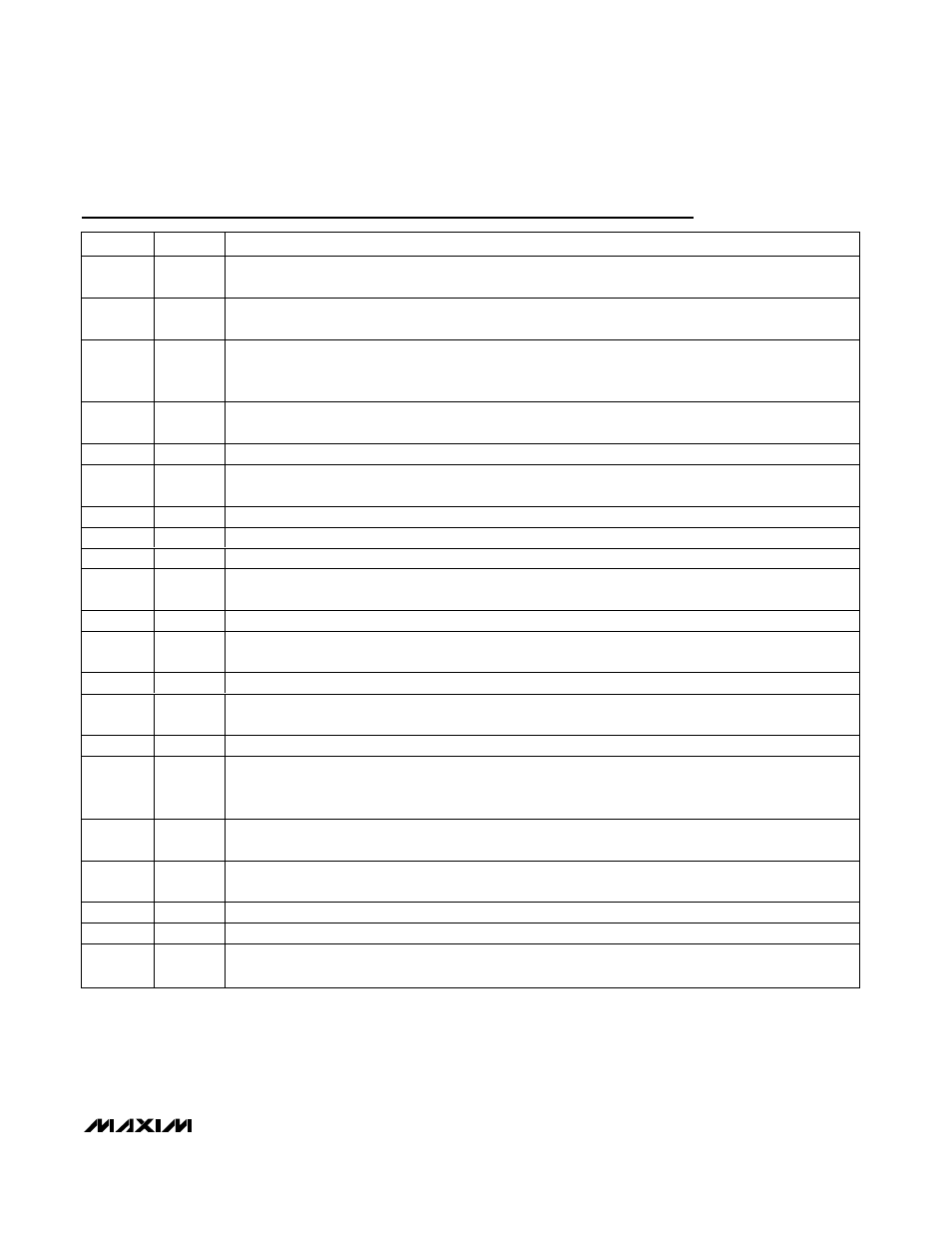
Pin Description
PIN
NAME
FUNCTION
1
REGOUT
Regulator Output. Always present as long as HVIN is powered with a voltage above UVLO threshold.
Bypass REGOUT to GND with a minimum 2.2µF ceramic capacitor.
2
RTCT
Oscillator Frequency Set Input. Connect a resistor from RTCT to REGOUT and a capacitor from RTCT to
GND to set the oscillator frequency.
3
FLTINT
Fault Integration Input. During persistent current-limit faults, a capacitor connected to FLTINT is charged
with an internal 80µA current source. Switching is terminated when V
FLTINT
reaches 2.7V. An external
resistor connected in parallel discharges the capacitor. Switching resumes when V
FLTINT
drops to 1.9V.
4
RCFF
Feed-Forward Input. To generate the PWM ramp, connect a resistor from RCFF to HVIN and a capacitor
from RCFF to GND.
5
RAMP
PWM Ramp Sense Input. Connect RAMP to RCFF.
6
OPTO
PWM Comparator Inverting Input. Connect the collector of the optotransistor to OPTO and a pullup resistor
to REGOUT.
7
CSS
Soft-Start and Reference. Connect a 10nF or greater capacitor from CSS to GND.
8
PPWM
PWM Pulse Output. PPWM leads the internal power MOSFET pulse by approximately 100ns.
9
GND
Signal Ground. Connect GND to PGND.
10
CS
Current-Sense Input. The current-limit threshold is internally set to 156mV relative to PGND. The device has
an internal noise filter. If necessary, connect an external RC filter for additional filtering.
11
PGND
Power Ground. Connect PGND to GND.
12
SRC
Internal Low-Side Power MOSFET Source. Connect SRC to PGND with a low-value resistor for current
limiting.
13
XFRMRL
Low-Side Connection for the Isolation Transformer
14
DRVIN
MOSFET Gate-Driver Supply Input. Bypass DRVIN with at least 0.1µF to PGND. Connect DRVIN to
REGOUT.
15
XFRMRH
High-Side Connection for the Isolation Transformer
16
DRNH
Drain Connection of the Internal High-Side PWM Power MOSFET. Connect DRNH to the most positive rail
of the input supply. Bypass DRNH appropriately to handle the heavy switching current through the
transformer.
17
BST
Boost Input. BST is the boost connection point for the high-side MOSFET driver. Connect a minimum
0.1µF capacitor from BST to XFRMRH with short and wide PC board traces.
18
UVLO
Undervoltage Lockout Input. Connect a resistive divider from HVIN to UVLO and from UVLO to GND to set
the UVLO threshold.
19
HVIN
High-Voltage Input. Connect HVIN to the most positive input supply rail.
20
INBIAS
Input from the Rectified Bias Winding. INBIAS is an input to the internal linear voltage regulator (REGOUT).
—
EP
Exposed Paddle. EP is internally connected to GND. Connect the exposed paddle to a copper pad to
improve power dissipation.