4v to 72v input ldos with boost preregulator – Rainbow Electronics MAX5093 User Manual
Page 20

MAX5092/MAX5093
Maximum Output Current (I
OUT_MAX
)
The MAX5092_/MAX5093_ high input voltage (+72V
max) provides up to 250mA of current from OUT.
Package power-dissipation limits the amount of output
current available for a given input/output voltage and
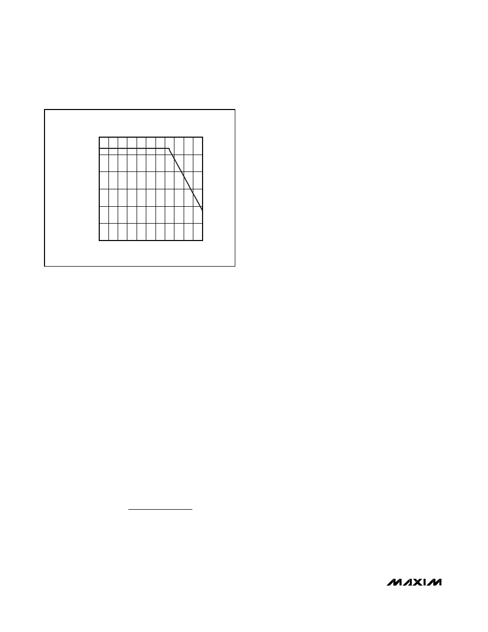
ambient temperature. Figure 8 depicts the maximum
power-dissipation curve for the devices. The graph
assumes that the exposed metal pad of the IC package
is soldered to the PC board copper according to the
JEDEC 51 standard (multilayer board). Use Figure 8 to
determine the allowable package dissipation for a
given ambient temperature. Alternately, use the follow-
ing formula to calculate the allowable package dissipa-
tion (P
DISS
) in watts:
For T
A
≤ +70°C:
P
DISS
= 2.67
For +70°C < T
A
≤ +125°C:
P
DISS
= 2.67 - (0.0333 x (T
A
- 70))
where +70°C < T
A
≤ +125°C and 0.0333W/°C is the
package thermal derating. After determining the allow-
able package dissipation, calculate the maximum out-
put current (I
OUT_MAX
) using the following formula:
where P
DISS
is the allowable package power dissipa-
tion and P
LOSS(BST)
is the boost converter power loss.
P
DISS
includes the losses in the boost converter opera-
tion and the LDO itself. The boost converter loss
P
LOSS(BST)
, depends on V
IN
, V
BSOUT
, and I
OUT
. See
the Boost Converter Power Loss graphs in the
Typical
Operating Characteristics
to estimate the losses at a
given V
IN
and V
BSOUT
at room temperature. At a higher
ambient temperature of +105°C, P
LOSS(BST)
increases
by up to 20% due to higher R
DS-ON
and switching loss-
es of the internal boost converter MOSFET. (Note:
I
OUT_MAX
must be less than 250mA).
PC Board Layout Guidelines
Good PC board (PCB) layout and routing are required
in high-frequency switching power supplies to achieve
proper regulation and stability. It is strongly recom-
mended that the evaluation kit PCB layouts be followed
as closely as possible. Refer to the MAX5092 EV kit for
an example layout. Follow these guidelines for good
PCB layout:
1) For SGND, use a large copper plane under the IC
and solder it to the exposed paddle. To effectively
use this copper area as a heat exchanger between
the PCB and ambient, expose this copper area on
the top and bottom side of the PCB. Do not make a
direct connection from the EP copper plane to pin 3
(SGND) underneath the IC so as to minimize
ground bounce.
2) Isolate the power components and high-current
path from the sensitive analog circuit.
3) Keep the high-current paths short, especially at the
ground terminals. This practice is essential for sta-
ble, jitter-free operation.
4) Connect the return terminals of input capacitors
and boost output capacitors to the PGND_BST
power ground plane. Connect the power ground
(PGND_BST) and signal ground (SGND) planes
together at the negative terminal of the input capac-
itors. Do not connect them anywhere else. Connect
PGND_LDO ground plane to SGND ground plane
at a single point.
5) Ensure that the feedback connections are short and
direct. Ensure a low-impedance path between
BSFB and SGND to limit the transient at BSFB to
100mV.
6) Route high-speed switching nodes away from the
sensitive analog areas. Use the internal PCB layer
for SGND as an EMI shield to keep radiated noise
away from the IC, feedback dividers, and bypass
capacitors.
I
P
P
V
V
OUT MAX
DISS
LOSS BST
IN
OUT
_
(
)
=
−
−
4V to 72V Input LDOs with Boost Preregulator
20
______________________________________________________________________________________
MAXIMUM POWER DISSIPATION
vs. AMBIENT TEMPERATURE
MAX5092/93 fig08
AMBIENT TEMPERATURE (°C)
MAXIMUM POWER DISSIPATION (W)
110
95
80
65
50
35
20
5
-10
-25
0.5
1.0
1.5
2.0
2.5
3.0
0
-40
125
Figure 8. MAX5092/MAX5093 Package Power Dissipation
