Max5480, Bit parallel dac in qsop-16 package, Detailed description – Rainbow Electronics MAX5480 User Manual
Page 4: Applications information, Table 1. mode-selection table, Interface-logic information
MAX5480
_______________Detailed Description
The MAX5480 is an 8-bit multiplying digital-to-analog
converter (DAC) that consists of a thin-film R-2R resistor
array with CMOS current steering switches. Figure 3
shows a simplified schematic of the DAC. The inverted
R-2R ladder divides the voltage or current reference in
a binary manner among the eight steering switches.
The magnitude of the current appearing at either OUT
terminal depends on the number of switches selected;
therefore, the output is an analog representation of the
digital input. The two OUT terminals must be held at the
same potential so a constant current is maintained in
each ladder leg. This makes the REF input current inde-
pendent of switch state and also ensures that the
MAX5480 maintains its excellent linearity performance.
Interface-Logic Information
Mode Selection
The inputs CS and WR control the MAX5480’s operat-
ing mode (see Table 1).
Write Mode
When CS and WR are both low, the MAX5480 is in write
mode, and its analog output responds to data activity at
the D0–D7 data-bus inputs. In this mode, the data
latches are transparent (see Tables 2 and 3).
Hold Mode
In hold mode, the MAX5480 retains the data that was
present on D0–D7 just prior to CS or WR assuming a
high state. The analog output remains at the value cor-
responding to the digital code locked in the data latch.
__________Applications Information
Using the MAX5480 in Voltage-
Output Mode (Single Supply)
The MAX5480 can be used either as a current-output
DAC (Figures 1 and 6) or as a voltage-output DAC
(Figures 2 and 5).
To use the MAX5480 in voltage mode, connect OUT1 to
the reference input and connect OUT2 to ground. REF,
now the DAC output, is a voltage source with a con-
stant output resistance of 10k
Ω
(nominally). This output
is often buffered with an op amp (Figure 5).
An advantage of voltage-mode operation is single-
supply operation for the complete circuit; i.e., a nega-
tive reference is not required for a positive output. It is
important to note that the range of the reference is
restricted in voltage mode. The reference input (voltage
at OUT1) must always be positive and is limited to no
more than V
DD
- 3V. If the reference voltage exceeds
this value, linearity is degraded.
8-Bit Parallel DAC in
QSOP-16 Package
4
_______________________________________________________________________________________
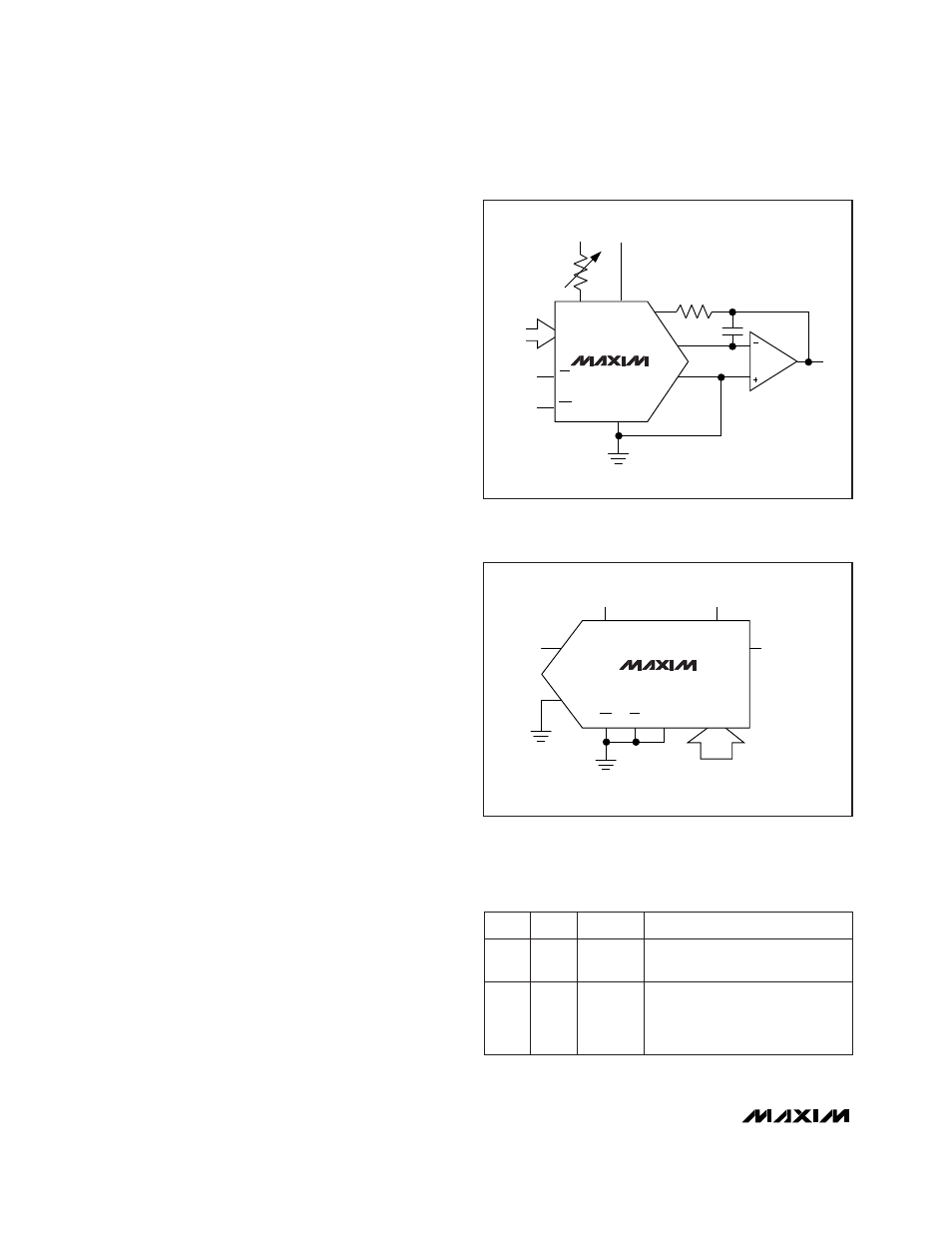
WR
L
L
H
X
X
H
CS
MAX5480
10pF
V
OUT
16
14
15
V
REF
V
DD
R2
1k
R1
2k
D7–D0
CS
OUT1
12
DATA
INPUTS 4–11
13
OUT2
1
2
WR
R1 AND R2 USED ONLY IF GAIN
ADJUSTMENT IS REQUIRED.
REF
R
FB
GND
3
V
DD
MAX4330
Figure 1. Unipolar Binary Operation (Two-Quadrant Multiplication)
MAX5480
REF
INPUT*
OUTPUT
VOLTAGE
(10k
Ω
OUTPUT
RESISTANCE)
OUT1
REF
14
15
1
2
16
13
12
3
OUT2
RFB
V
DD
+5V
GND
D7–D0
4–11
DATA IN
CS
WR
*(V
DD
- 3V, max)
Figure 2. Typical Operating Circuit (Voltage Mode—Unbuffered)
MODE
Write
Hold
Hold
DAC Response
DAC responds to data bus
(D0–D7) inputs.
Data bus (D0–D7) is locked out;
DAC holds last data present
when CS or WR assumed high
state.
Table 1. Mode-Selection Table
L = Low State, H = High State, X = Don’t Care