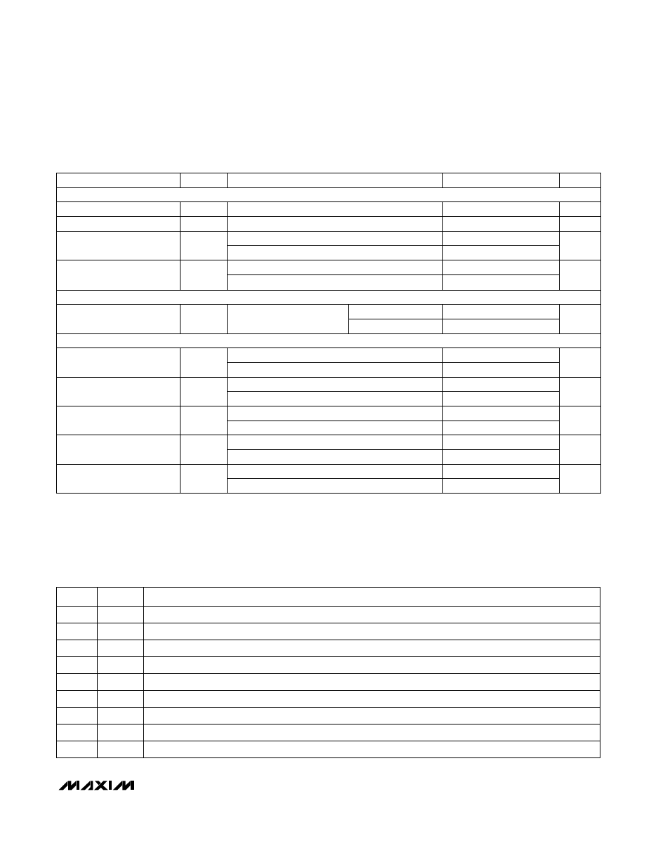
Pin description, Electrical characteristics (continued) – Rainbow Electronics MAX5480 User Manual
Page 3
MAX5480
8-Bit Parallel DAC in
QSOP-16 Package
_______________________________________________________________________________________
3
ELECTRICAL CHARACTERISTICS (continued)
(V
DD
= +5V, V
REF
= +10V, V
OUT1
= V
OUT2
= 0V, Circuit of Figure 1, T
A
= T
MIN
to T
MAX
, unless otherwise noted.)
Note 1:
Gain error is measured using internal feedback resistor. Full-scale range (FSR) = V
REF
.
Note 2:
Gain TempCo measured from +25°C to T
MAX
and from +25°C to T
MIN
.
Note 3:
Guaranteed by design.
Input Capacitance (Note 3)
C
IN
20
pF
8
WR, CS
D0–D7
T
A
= +25°C
PARAMETER
SYMBOL
MIN
TYP
MAX
UNITS
100
Supply Current
I
DD
500
Input Current
I
IN
±10
µA
±1
µA
T
A
= T
MIN
to T
MAX
Chip-Select to Write-
Setup Time
220
CONDITIONS
T
A
= T
MIN
to T
MAX
T
A
= +25°C; V
IN
= 0V to V
DD
Digital inputs at 0V or V
DD
MAX5480A
Input Low Voltage
V
IL
0.8
V
Input High Voltage
V
IH
2.4
V
ns
35
MAX5480B
t
CS
Chip-Select to Write-
Hold Time
0
MAX5480A
ns
0
MAX5480B
t
CH
Write Pulse Width
220
MAX5480A
ns
35
MAX5480B
t
WR
Data-Setup Time
170
MAX5480A
ns
55
MAX5480B
t
DS
Data-Hold Time
10
MAX5480A
ns
-7
MAX5480B
t
DH
POWER REQUIREMENTS
SWITCHING CHARACTERISTICS
(Figure 4)
DIGITAL INPUTS
______________________________________________________________Pin Description
NAME
FUNCTION
1
OUT1
R-2R Ladder Output
PIN
2
OUT2
R-2R Ladder Output, complement of OUT1
3
GND
Ground
4–11
D7–D0
Data Inputs, D7 is the most significant bit.
12
CS
Chip Select Input. Active Low.
13
WR
Write Control Input. Active Low.
14
V
DD
Power Supply Input, +5V
15
REF
Reference Voltage Input
16
RFB
Feedback Resistor Connection