Rainbow Electronics MAX31723 User Manual
Page 12
MAX31722/MAX31723
Digital Thermometers and Thermostats
with SPI/3-Wire Interface
12
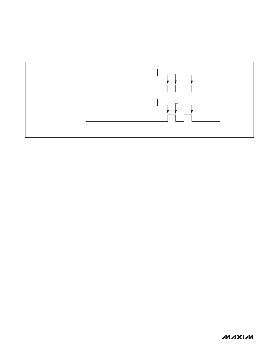
Figure 7. Serial Clock as a Function of Microcontroller Clock Polarity (CPOL)
Address and Data Bytes
Address and data bytes are shifted MSB first into the
serial-data input (SDI) and out of the serial-data output
(SDO). Any transfer requires the address of the byte to
specify a write or a read, followed by one or more bytes of
data. Data is transferred out of the SDO for a read opera-
tion and into the SDI for a write operation. The address
byte is always the first byte entered after CE is driven
high. The MSB (A7) of this byte determines if a read or
write takes place. If A7 is 0, one or more read cycles
occur. If A7 is 1, one or more write cycles occur.
Data transfers can occur 1 byte at a time in multiple-byte
burst mode. After CE is driven high, an address is writ-
ten to the devices. After the address, one or more data
bytes can be written or read. For a single-byte transfer,
1 byte is read or written and then CE is driven low (see
Figures 8 and 9). For a multiple-byte transfer, however,
multiple bytes can be read or written to the devices
after the address has been written (see Figure 10). A
single-byte burst read/write sequentially points through
all memory locations and loops from 7Fh/FFh to 00h/80h.
Invalid memory addresses report an FFh value.
3-Wire Serial-Data Bus
The 3-wire communication mode operates similarly to
the SPI mode. However, in 3-wire mode, there is one
bidirectional I/O instead of separate data-in and data-
out signals. The 3-wire consists of the I/O (SDI and
SDO pins connected together), CE, and SCLK pins. In
3-wire mode, each byte is shifted in LSB first, unlike SPI
mode where each byte is shifted in MSB first. As is the
case with the SPI mode, an address byte is written to
the devices followed by a single data byte or multiple
data bytes. Figure 11 illustrates a read and write cycle.
Figure 12 illustrates a multiple-byte burst transfer. In
3-wire mode, data is input on the rising edge of SCLK
and output on the falling edge of SCLK.
CE
SHIFT
SHIFT
INTERNAL STROBE
INTERNAL STROBE
CPOL = 1
CPOL = 0
SCLK
CE
SCLK
NOTE: CPOL IS A BIT THAT IS SET IN THE MICROCONTROLLER’S CONTROL REGISTER.