Serial interface – Rainbow Electronics MAX31723 User Manual
Page 11
MAX31722/MAX31723
Digital Thermometers and Thermostats
with SPI/3-Wire Interface
11
as depicted in the AC Electrical Characteristics. The user
has read/write access to the R1 and R0 bits, which are
nonvolatile. See Table 4.
Serial Interface
The devices offer the flexibility to choose between two
serial interface modes. They can communicate with the
SPI interface or with a 3-wire interface. The interface
method used is determined by the SERMODE pin. When
SERMODE is connected to V
DD
, SPI communication
is selected. When SERMODE is connected to ground,
3-wire communication is selected.
Serial Peripheral Interface (SPI)
The SPI is a synchronous bus for address and data
transfer. The SPI mode of serial communication is select-
ed by connecting SERMODE to V
DD
. Four pins are used
for the SPI: SDO (serial-data out), SDI (serial-data in), CE
(chip enable), and SCLK (serial clock). The devices are
the slave device in an SPI application, with the microcon-
troller being the master. SDI and SDO are the serial-data
input and output pins for the devices, respectively. The
CE input is used to initiate and terminate a data transfer.
SCLK is used to synchronize data movement between
the master (microcontroller) and the slave (IC) devices.
The serial clock (SCLK), which is generated by the
microcontroller, is active only when CE is high and dur-
ing address and data transfer to any device on the SPI
bus. The inactive clock polarity is programmable in some
microcontrollers. The devices offer an important feature
in that the level of the inactive clock is determined by
sampling SCLK when CE becomes active. Therefore,
either SCLK polarity can be accommodated. Input data
(SDI) is latched on the internal strobe edge and output
data (SDO) is shifted out on the shift edge (see Table 5
and Figure 7). There is one clock for each bit transferred.
Address and data bits are transferred in groups of eight,
MSB first.
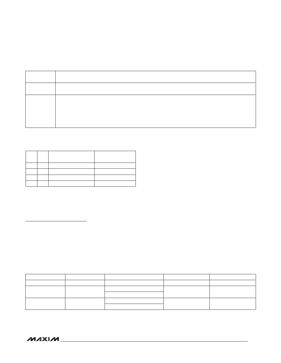
Table 3. Configuration/Status Register Bit Descriptions (continued)
Table 5. Function Table
Table 4. Thermometer Resolution
Configuration
Note: CPHA bit polarity must be set to 1.
*CPOL is the clock polarity bit that is set in the control register of the microcontroller.
**SDO remains at high impedance until 8 bits of data are ready to be shifted out during a read.
BIT 2
R1: Thermostat resolution bit 1. Factory power-up state = 0 and is stored in nonvolatile memory. Sets the con-
version resolution (see Table 4).
BIT 1
R0: Thermostat resolution bit 0. Factory power-up state = 0 and is stored in nonvolatile memory. Sets the con-
version resolution (see Table 4).
BIT 0
SD: Factory power-up state = 1. The user has read/write access to the SD bit, which is stored in nonvolatile
memory.
0 = The devices continuously perform temperature conversions and store the last completed result in the tem-
perature register.
1 = The conversion in progress is completed and stored, and then the devices revert to a low-power shutdown
mode. The communication port remains active.
R1
R0
THERMOMETER
RESOLUTION (BITS)
MAX CONVERSION
TIME (ms)
0
0
9
25
0
1
10
50
1
0
11
100
1
1
12
200
MODE
CE
SCLK
SDI
SDO
Disable reset
Low
Input disabled
Input disabled
High impedance
Write
High
CPOL = 1*, SCLK rising
Data bit latch
High impedance
CPOL = 0, SCLK falling
Read
High
CPOL = 1, SCLK falling
X
Next data bit shift**
CPOL = 0, SCLK rising