Max4895e, Vga port protector, Applications information – Rainbow Electronics MAX4895E User Manual
Page 4: Detailed description, Pin description
MAX4895E
Applications Information
The MAX4895E provides the level shifting necessary to
drive two standard VGA ports from a graphics controller
as low as +2.2V. Internal buffers drive the HSYNC and
VSYNC signals to VGA standard TTL levels. The DDC
switch provides level shifting by clamping signals to a
diode drop less than V
L
(see the
Typical Operating
Circuit
). Connect V
L
to +3.3V for normal operation.
Power-Supply Decoupling
Bypass V
CC
and V
L
to ground with a 1µF ceramic
capacitor as close as possible to the device.
PCB Layout
High-speed switches such as the MAX4895E require
proper PCB layout for optimum performance. Ensure
that impedance-controlled PCB traces for high-speed
signals are matched in length and are as short as pos-
sible. Connect the exposed pad to a solid ground
plane.
Detailed Description
The MAX4895E integrates level-translating buffers and
features R, G, B port protection for VGA signals.
Horizontal and vertical synchronization (H0/V0) inputs
feature level-shifting buffers to support low-voltage
CMOS or standard TTL-compatible graphics con-
trollers. The device meets ±10µA VESA drive require-
ments. The MAX4895E also features I
2
C level shifting
using two nMOS devices. All outputs maintain ±15kV
Human Body Model (HBM) and ±8kV Contact
Discharge per IEC 61000-4-2 on seven terminals
(SDA1, SCL1, H1, V1, R, G, B). The R, G, B pads pro-
tect the digital-to-analog converter (DAC) and are sim-
ply placed in parallel with the R, G, B outputs for the
DAC and VGA socket.
VGA Port Protector
4
_______________________________________________________________________________________
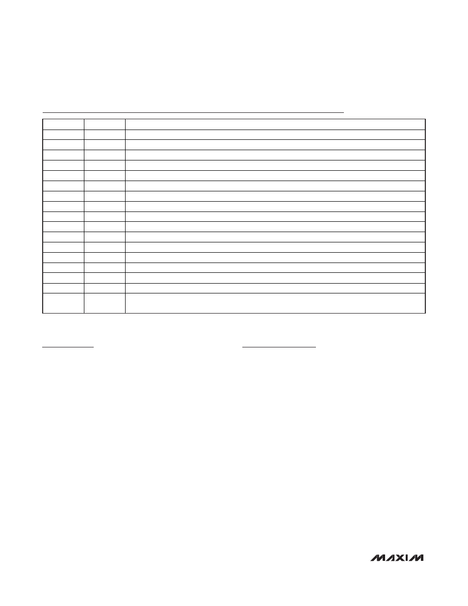
Pin Description
PIN
NAME
FUNCTION
1
R
High-ESD Protection Diodes for RGB Signals
2
G
High-ESD Protection Diodes for RGB Signals
3
B
High-ESD Protection Diodes for RGB Signals
4 GND
Ground
5 V
L
Supply Voltage, +2.0V to V
CC
. Bypass V
L
to GND with a 1μF ceramic capacitor.
6
N.C.
No Connection. Leave unconnected.
7
SDA0
SDA I/O. SDA0 referenced to V
L
.
8
SDA1
SDA I/O. SDA1 referenced to V
CC
.
9
SCL0
SCL I/O. SCL0 referenced to V
L
.
10
SCL1
SCL I/O. SCL1 referenced to V
CC
.
11
H0
Horizontal Sync Input
12
H1
Horizontal Sync Output
13 V0
Vertical
Sync
Input
14
V1
Vertical Sync Output
15 V
CC
Power-Supply Voltage, +4.5V to +5.5V. Bypass V
CC
to GND with a 1μF ceramic capacitor.
16
EN
Enable for H1 and V1 Outputs
— EP
Exposed Pad. Connect EP to GND or leave unconnected. For enhanced thermal dissipation,
connect EP to a copper area as large as possible. Do not use EP as a sole ground connection.