Rainbow Electronics MAX14523C User Manual
Page 2
MAX14523A/MAX14523AL/MAX14523B/MAX14523C
250mA to 1.5A, Adjustable
Current-Limit Switches
2
_______________________________________________________________________________________
ABSOLUTE MAXIMUM RATINGS
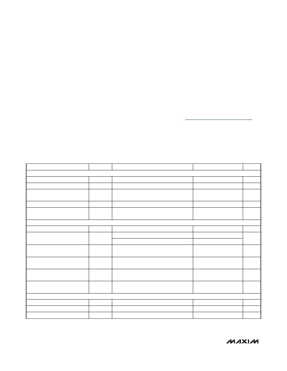
ELECTRICAL CHARACTERISTICS
(V
IN
= +1.7V to +5.5V, R
SETI
= 94.2k
Ω, C
IN
= C
OUT
= 1µF, and T
A
= T
J
= -40°C to +125°C, unless otherwise noted. Typical values
are at V
IN
= +3.3V, T
A
= +25°C.) (Note 2)
Stresses beyond those listed under “Absolute Maximum Ratings” may cause permanent damage to the device. These are stress ratings only, and functional
operation of the device at these or any other conditions beyond those indicated in the operational sections of the specifications is not implied. Exposure to
absolute maximum rating conditions for extended periods may affect device reliability.
Note 1: Package thermal resistances were obtained using the method described in JEDEC specification JESD51-7, using a four-
layer board. For detailed information on package thermal considerations, refer to
www.maxim-ic.com/thermal-turorial
.
(All voltages referenced to GND.)
IN, ON, ON, FLAG, OUT, and SETI to GND .............-0.3V to +6V
Current into Any Pin (Except IN, OUT)................................20mA
Out Short Circuit to GND...................................Internally Limited
Continuous Power Dissipation (T
A
= +70°C) for multilayer board:
8-Pin TDFN (derate 24.4mW/°C above +70°C) .........1952mW
Junction-to-Case Thermal Resistance (
θ
JC
)
(Note 1) ...................................................................8.0°C/W
Junction-to-Ambient Thermal Resistance (
θ
JA
)
(Note 1) .................................................................41.0°C/W
Operating Temperature Range .........................-40°C to +125°C
Junction Temperature ......................................................+150°C
Storage Temperature Range .............................-65°C to +150°C
Lead Temperature (soldering, 10s) .................................+300°C
PARAMETER
SYMBOL
CONDITIONS
MIN
TYP
MAX
UNITS
SUPPLY OPERATION
Operating Voltage
V
IN
1.7
5.5 V
Quiescent Current
I
Q
I
OUT
= 0A, switch on, V
IN
= 3.3V
170
300
μA
Latchoff Current
I
LATCH
V
IN
= 3.3V, I
OUT
= 0A , after an overcurrent
fault (MAX14523B)
10
20
μA
Shutdown Forward Current
I
SHDN
V
ON
= 0V, V
ON
= V
IN
, V
IN
= 5.5V, V
OUT
= 0V
0.5
7
μA
Shutdown Reverse Current
I
RSHDN
V
ON
= 0V, V
ON
= V
IN
, V
IN
= 1.7V, V
OUT
=
5.5V (current into OUT)
0.01
0.6 μA
INTERNAL FET
Switch-On Resistance
R
ON
V
IN
= 3.3V, I
OUT
lower than I
LIM
70 130 m
R
SETI
= 91.78k
, V
IN
- V
OUT
=
1V
1350 1500 1650
Forward-Current Limit
I
LIM
R
SETI
= 563.12k
, V
IN
- V
OUT
= 1V
225
250
275
mA
(R
SETI
+2.48k
) × I
LIM
Product
I
LIM
= 250mA to 1500mA,
V
IN
- V
OUT
= 1V
127.2 141.4 155.5
kV
Reverse Blocking Current
V
OUT
> V
IN
+ 140mV, after reverse-current-
limit shutdown
2
μA
Reverse Blocking Threshold
V
OUT
- V
IN
V
OUT
- V
IN
= 300mV, OUT falling until
switch turns on
40 95 140 mV
FLAG Assertion Drop Voltage
Threshold
V
FA
Increase (V
IN
- V
OUT
) drop until
FLAG
asserts, I
OUT
limiting, V
IN
= 3.3V
350 mV
ON,
ON INPUT
ON,
ON Input Leakage
I
LEAK
V
ON
, V
ON
= V
IN
or V
GND
-1
+1
μA
ON,
ON Input Logic-High Voltage
V
IH
1.6
V
ON,
ON Input Logic-Low Voltage
V
IL
0.4
V