Chip information, Package information, Pin configuration – Rainbow Electronics MAX14523C User Manual
Page 10
MAX14523A/MAX14523AL/MAX14523B/MAX14523C
250mA to 1.5A, Adjustable
Current-Limit Switches
Maxim cannot assume responsibility for use of any circuitry other than circuitry entirely embodied in a Maxim product. No circuit patent licenses are
implied. Maxim reserves the right to change the circuitry and specifications without notice at any time.
10 ____________________Maxim Integrated Products, 120 San Gabriel Drive, Sunnyvale, CA 94086 408-737-7600
© 2009 Maxim Integrated Products
Maxim is a registered trademark of Maxim Integrated Products, Inc.
Do not use an R
SETI
value smaller than 91.78k
Ω.
Note: Connecting any capacitance larger than 20pF to
SETI can cause instability.
IN Bypass Capacitor
Connect a minimum of 1µF capacitor from IN to GND to
limit the input voltage drop during momentary output
short-circuit conditions. Larger capacitor values further
reduce the voltage undershoot at the input.
OUT Bypass Capacitor
For stable operation over the full temperature range
and over the full-programmable current-limit range, use
a 1µF ceramic capacitor from OUT to ground.
Excessive output capacitance can cause a false over-
current condition due to decreased dv/dt across the
capacitor. Calculate the maximum capacitive load
(C
MAX
) value that can be connected to OUT using the
following formula:
For example, for V
IN
= 3.3V, t
BLANK
= 10ms, and I
LIM
=
300mA, C
MAX
equals 909µF.
Layout and Thermal Dissipation
To optimize the switch response time to output short-
circuit conditions, it is very important to keep all traces
as short as possible to reduce the effect of undesirable
parasitic inductance. Place input and output capacitors
as close as possible to the device (no more than 5mm).
IN and OUT must be connected with wide short traces
to the power bus. During normal operation, the power
dissipation is small and the package temperature
change is minimal. If the output is continuously shorted
to ground at the maximum supply voltage, the opera-
tion of the switches with the autoretry option does not
cause problems because the total power dissipated
during the short is scaled by the duty cycle:
Attention must be given to the MAX14523C continuous
current-limit version when the power dissipation during
a fault condition can cause the device to reach the ther-
mal shutdown threshold.
Chip Information
PROCESS: BiCMOS
P
V
I
t
t
t
MAX
IN MAX
OUT MAX
BLANK
RETRY
BLA
(
)
(
)
(
)
=
Ч
Ч
+
N
NK
C
µF
I
mA
t
ms
V
V
MAX
LIM
BLANK MIN
IN
(
)
(
)
(
)
( )
(
)
=
×
R
SETI
(k
)
TYPICAL CURRENT LIMIT/THRESHOLD (mA)
91.78 1500
121 1145
221 632
301 466
422 333
563.12 250
(Open)
0
Table 2. Current Limit/Threshold vs.
Resistor Values
PACKAGE TYPE
PACKAGE CODE
DOCUMENT NO.
8 TDFN-EP
T833+2
Package Information
For the latest package outline information and land patterns, go to
www.maxim-ic.com/packages
.
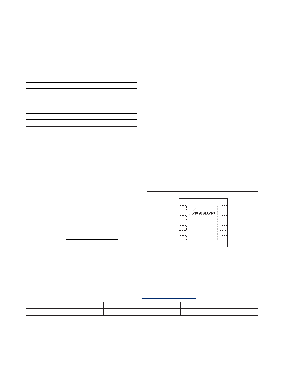
Pin Configuration
MAX14523A
MAX14523AL
MAX14523B
MAX14523C
1
+
TDFN
3mm x 3mm
N.C.
2
FLAG
3
SETI
4
OUT
8
GND
7
ON(ON)**
6
N.C.
5
IN
*CONNECT EXPOSED PAD TO GND.
**( ) FOR THE MAX14523AL ONLY.
*EP