Rainbow Electronics MAX15010 User Manual
Page 2
MAX15008/MAX15010
Automotive 300mA LDO Voltage Regulators
with Tracker Output and Overvoltage Protector
2
_______________________________________________________________________________________
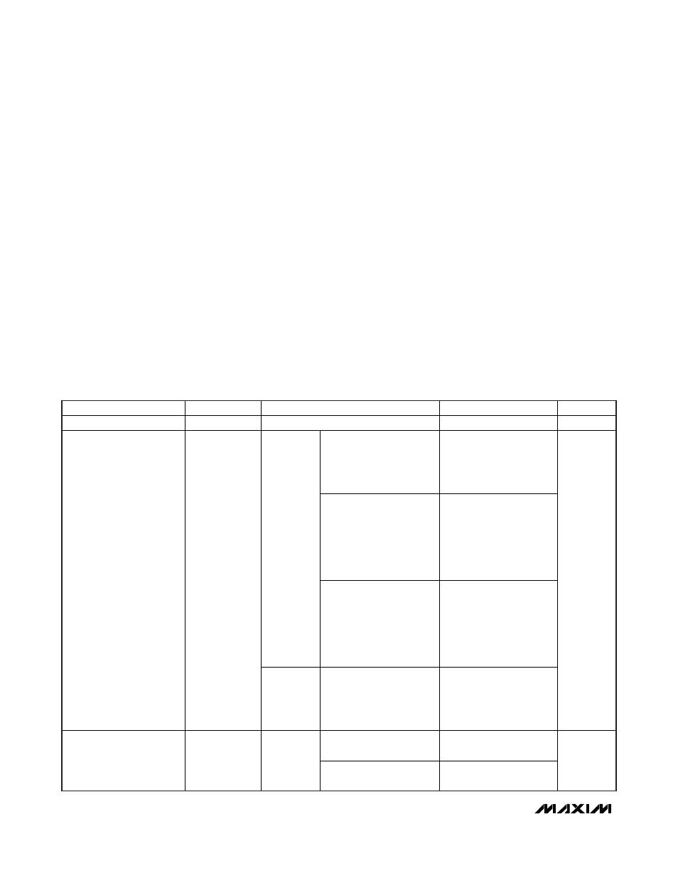
ABSOLUTE MAXIMUM RATINGS
ELECTRICAL CHARACTERISTICS
(V
IN
= V
TRACK
= +14V, V
SGND
= V
PGND
= 0V, C
GATE
= 6000pF, C
IN
= 10µF (ESR ≤ 1.5Ω), C
OUT_LDO
= 22µF (ceramic), C
TRACK
=
3.3µF (ceramic) (ESR ≤ 1.5Ω), C
OUT_TRK
= 10µF (ESR ≤ 1.5Ω), C
REF
= 1000pF, V
OUT_LDO
= 5V, T
A
= T
J
= -40°C to +125°C, unless
otherwise noted. Typical values are at T
A
= +25°C.) (Note 1)
Stresses beyond those listed under “Absolute Maximum Ratings” may cause permanent damage to the device. These are stress ratings only, and functional
operation of the device at these or any other conditions beyond those indicated in the operational sections of the specifications is not implied. Exposure to
absolute maximum rating conditions for extended periods may affect device reliability.
(All pins referenced to SGND, unless otherwise noted.)
IN, GATE.................................................................-0.3V to +45V
TRACK.....................................................................-20V to +45V
EN_LDO, EN_PROT, EN_TRK .....................-0.3V to (V
IN
+ 0.3V)
SOURCE ......................................................-0.3V to (V
IN
+ 0.3V)
TRACK to OUT_TRK................................................-40V to +40V
OUT_TRK, FB_TRK, ADJ...........................................-5V to +45V
OUT_LDO, FB_LDO, FB_PROT, RESET.................-0.3V to +12V
GATE to SOURCE ..................................................-0.3V to +12V
HOLD................................................-0.3V to (V
OUT_LDO
+ 0.3V)
REF to SGND............................................................-0.3V to +6V
CT to SGND............................................................-0.3V to +12V
SGND to PGND .....................................................-0.3V to +0.3V
IN, OUT_LDO Current .......................................................700mA
TRACK, OUT_TRK Current ...............................................350mA
Current Sink/Source (all remaining pins) ............................50mA
Continuous Power Dissipation (T
A
= +70°C)
32-Pin TQFN (derate 34.5mW/°C above +70°C) .............2.7W*
Thermal Resistance
θ
JA
..............................................................................29.0°C/W
θ
JC
................................................................................1.7°C/W
Operating Temperature Range .........................-40°C to +125°C
Junction Temperature ......................................................+150°C
Storage Temperature Range .............................-60°C to +150°C
Lead Temperature (soldering, 10s) .................................+300°C
PARAMETER
SYMBOL
CONDITIONS
MIN
TYP
MAX
UNITS
Supply Voltage Range
V
IN
5
40
V
EN_LDO = IN, EN_TRK =
EN_PROT = 0V, I
OUT_LDO
= 0µA, LDO on, tracker
off, protector off,
measured from SGND
67
85
EN_LDO = EN_TRK = IN,
EN_PROT = 0V, LDO on,
I
OUT_LDO
= 100µA, tracker
on, I
OUT_TRK
= 0µA,
protector off, V
FB_TRK
=
V
OUT_TRK
, V
ADJ
= V
REF,
measured from SGND
120
180
MAX15008
EN_LDO = EN_TRK =
EN_PROT = IN, LDO on,
I
OUT_LDO
= 100µA, tracker
on, I
OUT_TRK
= 0µA,
protector on, V
FB_TRK
=
V
OUT_TRK
;
V
ADJ
= V
REF,
measured from SGND
190
280
Supply Current
I
IN
MAX15010
EN_LDO = EN_TRK = IN,
LDO on, I
OUT_LDO
=
100µA, tracker on,
I
OUT_TRK
= 0µA,
measured from SGND
115
160
µA
T
A
= -40°C to +85°C
16
30
Shutdown Supply Current
I
SHDN
E N _LD O =
E N _P ROT =
EN_TRK = 0V,
measured
from SGND
T
A
= -40°C to +125°C
40
µA
*
As per JEDEC51 Standard, Multilayer Board (PCB).