Setting the reset timeout period, Tracker input/feedback adjustment, Electrical characteristics – Rainbow Electronics MAX15010 User Manual
Page 16
MAX15008/MAX15010
Setting the
RESET Timeout Period
The reset timeout period is adjustable to accommodate
a variety of applications. Set the reset timeout period by
connecting a capacitor, C
RESET
, between CT and
SGND. Use the following formula to select the reset
timeout period, t
RESET
:
t
RESET
= C
RESET
x V
CT_TH
/ I
CT
where t
RESET
is in seconds and C
RESET
is in µF.
V
CT_TH
is the CT ramp threshold in volts and I
CT
is the
CT ramp current in µA, as described in the
Electrical
Characteristics
table.
Leave CT open to select an internally fixed timeout peri-
od of 10µs. To maintain reset timeout accuracy, use a
low-leakage (< 10nA) type capacitor.
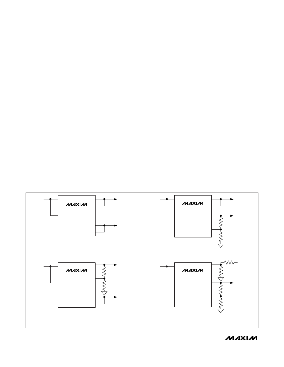
Tracker Input/Feedback Adjustment
The tracker can be powered from the LDO input supply
voltage or an independent voltage source. It is
designed to supply power to a remote sensor and its
supply input, TRACK, is able to handle the severe con-
ditions in automotive applications such as battery
reversal and load-dump transients up to 45V.
The tracker feedback, FB_TRK, and a separate tracker
reference voltage input, ADJ, offer the flexibility of set-
ting the tracker output to be lower, equal to, or higher
than the main (LDO) output. Other external voltages
can also be tracked.
Connect ADJ to OUT_LDO and FB_TRK to OUT_TRK to
track the LDO output voltage directly (Figure 4a). To
track a voltage higher than V
OUT_LDO
, directly connect
ADJ to OUT_LDO and connect FB_TRK to OUT_TRK
through a resistive voltage-divider (Figure 4b). To track
a voltage lower than the LDO regulator output,
V
OUT_LDO
, directly connect FB_TRK to OUT_TRK and
connect ADJ to OUT_LDO through a resistive voltage-
divider (Figure 4c). To track an external voltage V
X
with
a generic attenuation/amplification ratio, connect resis-
tive voltage-dividers between ADJ and the voltage input
or output to be tracked (V
X
), and between OUT_TRK
and FB_TRK (Figure 4d). Pay attention to the resistive
loading of the voltage V
X
due to the divider R5, R6.
To track the internal REF voltage (1.235V), directly connect
ADJ to REF. The voltage at FB_TRK or ADJ should be
greater than or equal to 1.1V and less than V
TRACK
- 0.5V.
Resistors should have a tolerance of 1% or better. Their
values should be low enough to ensure that the divider
current is at least 100x the maximum input bias current
at pins FB_TRK and ADJ (I
FB_TRK_ADJ
, max = 0.2µA).
Automotive 300mA LDO Voltage Regulators
with Tracker Output and Overvoltage Protector
16
______________________________________________________________________________________
IN
LDO
OUTPUT
V
IN
OUT_TRK
OUT_LDO
TRACKER
OUTPUT
FB_TRK
ADJ
MAX15008
MAX15010
TRACK
IN
LDO
OUTPUT
R3
V
IN
OUT_TRK
OUT_LDO
TRACKER
OUTPUT
ADJ
MAX15008
MAX15010
R4
FB_TRK
R5
R6
R6
TRACK
TO TRACK V
OUT_LDO
:
V
OUT_TRK
= V
OUT_LDO
TO TRACK A VOLTAGE HIGHER THAN
V
OUT_LDO
:
V
OUT_TRK
= V
OUT_LDO
x (R3 + R4) / R4,
R3 + R4 < V
OUT_TRK
/ 20
μA
(a)
(b)
IN
LDO
OUTPUT
V
IN
OUT_TRK
OUT_LDO
TRACKER
OUTPUT
FB_TRK
ADJ
MAX15008
MAX15010
TRACK
IN
R3
V
IN
OUT_TRK
ADJ
TRACKER
OUTPUT
MAX15008
MAX15010
R4
FB_TRK
TRACK
TO TRACK A VOLTAGE LOWER THAN V
OUT_LDO
:
V
OUT_TRK
= V
OUT_LDO
x R6 / (R5 + R6),
R5 + R6 < V
OUT_LDO
/ 20
μA
TO TRACK A GENERIC VOLTAGE V
X
:
V
OUT_TRK
= V
X
x (R6 / (R5 + R6)) x ((R3 + R4) / R4),
R5 + R6 < V
X
/ 20
μA, R3 + R4 < V
OUT_TRK
/ 20
μA
R5
(c)
(d)
V
X
Figure 4. Tracker Input and Feedback Adjustment