Rainbow Electronics MAX15010 User Manual
Page 18
MAX15008/MAX15010
External MOSFET Selection
Select the external MOSFET with adequate voltage
rating, V
DSS
, to withstand the maximum expected load-
dump input voltage. The on-resistance of the MOSFET,
R
DS(ON)
, should be low enough to maintain a minimal
voltage drop at full load, limiting the power dissipation
of the MOSFET.
During regular operation, the power dissipated by the
MOSFET is:
P
NORMAL
= I
LOAD
2
x R
DS(ON)
Normally, this power loss is small and is safely handled
by the MOSFET. However, when operating the
MAX15008 in overvoltage-limiter mode under pro-
longed or frequent overvoltage events, select an exter-
nal MOSFET with an appropriate power rating.
During an overvoltage event, the power dissipation in
the external MOSFET is proportional to both load cur-
rent and to the drain-source voltage, resulting in high
power dissipated in the MOSFET (Figure 7). The power
dissipated across the MOSFET is:
P
OV_LIMITER
= V
Q1
x I
LOAD
where V
Q1
is the voltage across the MOSFET’s drain
and source during overvoltage-limiter operation, and
I
LOAD
is the load current.
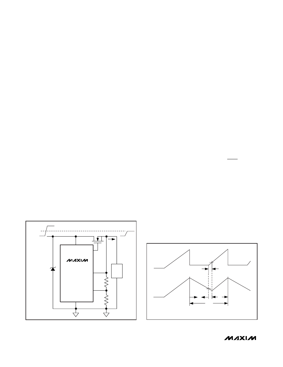
Overvoltage-Limiter Mode
Switching Frequency
When the MAX15008 is configured in overvoltage-
limiter mode, the external n-channel MOSFET is subse-
quently switched on and off during an overvoltage
event. The output voltage at SOURCE resembles a
periodic sawtooth waveform. Calculate the period of
the waveform, t
OVP
, by summing three time intervals
(Figure 8):
t
OVP
= t
1
+ t
2
+ t
3
where t
1
is the V
SOURCE
output discharge time, t
2
is the
GATE delay time, and t
3
is the V
SOURCE
output charge time.
During an overvoltage event, the power dissipated
inside the MAX15008 is due to the gate pulldown cur-
rent, I
GATEPD
. This amount of power dissipation is
worse when I
SOURCE
= 0 (C
SOURCE
is discharged only
by the internal current sink).
The worst-case internal power dissipation contribution
in overvoltage-limiter mode, P
OVP
, in watts can be
approximated using the following equation:
where V
OV
is the overvoltage threshold voltage in volts
and I
GATEPD
is the 63mA (typ) GATE pulldown current.
Output Discharge Time (t
1
)
When the voltage at SOURCE exceeds the adjusted
overvoltage threshold, GATE’s internal pulldown is
enabled until V
SOURCE
drops by 4%. The internal cur-
rent sink, I
GATEPD
, and the external load current,
I
LOAD
, discharge the external capacitance from
SOURCE to ground.
P
V
I
t
t
OVP
OV
GATEPD
OVP
=
Ч
Ч
Ч
0 98
1
.
Automotive 300mA LDO Voltage Regulators
with Tracker Output and Overvoltage Protector
18
______________________________________________________________________________________
t
2
t
1
t
OVP
t
3
GATE
SOURCE
Figure 8. MAX15008 Timing Diagram
IN
FB_PROT
SGND
GATE
SOURCE
TVS
MAX15008
LOAD
I
LOAD
+ V
Q1
-
V
SOURCE
V
SOURCE
V
OV
V
MAX
Figure 7. Power Dissipated Across MOSFETs During an
Overvoltage Fault (Overvoltage Limiter Mode)