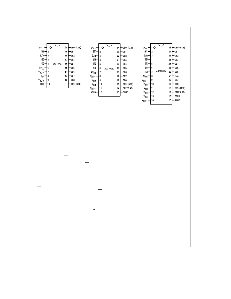
Connection diagrams, Pin descriptions – Rainbow Electronics ADC10064 User Manual
Page 9

Connection Diagrams
Dual-In-Line Package
TL H 11020 – 11
Top View
Dual-In-Line Package
TL H 11020 – 12
Top View
Dual-In-Line Package
TL H 11020 – 13
Top View
Pin Descriptions
DV
CC
AV
CC
These are the digital and analog positive sup-
ply voltage inputs They should always be
connected to the same voltage source but
are brought out separately to allow for sepa-
rate bypass capacitors
Each supply pin
should be bypassed with a 0 1 mF ceramic
capacitor in parallel with a 10 mF tantalum
capacitor to ground
INT
This is the active low interrupt output INT
goes low at the end of each conversion and
returns to a high state following the rising
edge of RD
S H
This is the Sample Hold control input When
this pin is forced low (and CS is low) it caus-
es the analog input signal to be sampled and
initiates a new conversion
RD
This is the active low Read control input
When this RD and CS are low any data pres-
ent in the output registers will be placed on
the data bus
CS
This is the active low Chip Select control in-
put When low this pin enables the RD and
S H pins
S0 S1
On the multiple-input devices (ADC10062
and ADC10064) these pins select the analog
input that will be connected to the A D during
the conversion The input is selected based
on the state of S0 and S1 when S H makes
its High-to-Low transition (See the Timing Di-
agrams) The ADC10064 includes both S0
and S1 The ADC10062 includes just S0 and
the ADC10061 includes neither
V
REF
b
These are the reference voltage inputs They
V
REF
a
may be placed at any voltage between GND
and V
CC
but V
REF
a
must be greater than
V
REF
b
An input voltage equal to V
REF
b
produces an output code of 0 and an input
voltage equal to (V
REF
a
b
1 LSB) produces
an output code of 1023
V
IN
V
IN0
These are the analog input pins
The
V
IN1
V
IN2
ADC10061
has
one
input
(V
IN
)
the
V
IN3
ADC10062 has two inputs (V
IN0
and V
IN1
)
and the ADC10064 has four inputs (V
IN0
V
IN1
V
IN2
and V
IN3
) The impedance of the
source should be less than 500X for best ac-
curacy and conversion speed For accurate
conversions no input pin (even one that is
not selected) should be driven more than
50 mV above V
CC
or 50 mV below ground
GND AGND These are the power supply ground pins The
DGND
ADC10061 has a single ground pin (GND)
and the ADC10062 and ADC10064 have sep-
arate analog and digital ground pins (AGND
and DGND) for separate bypassing of the an-
alog and digital supplies The ground pins
should be connected to a stable noise-free
system ground For the devices with two
ground pins both pins should be returned to
the same potential
DB0 – DB9
These are the TRI-STATE output pins
SPEED ADJ
(ADC10062 and ADC10064 only) This pin is
normally left unconnected but by connecting
a resistor between this pin and ground the
conversion time can be reduced See the
Typical Performance Curves and the table of
Electrical Characteristics
9
