Ac electrical characteristics – Rainbow Electronics ADC10064 User Manual
Page 4
AC Electrical Characteristics
(Continued)
The following specifications apply for V
a
e
a
5V t
r
e
t
f
e
20 ns V
REF(
a
)
e
5V V
REF(
b
)
e
GND and Speed Adjust pin
unconnected unless otherwise specified Boldface limits apply for T
A
e
T
J
e
T
MIN
to T
MAX
all other limits T
A
e
T
J
e
a
25 C
Symbol
Parameter
Conditions
Typical
Limit
Units
(Note 7)
(Note 8)
(Limits)
t
MS
Multiplexer Control Setup Time
10
75
ns (max)
t
MH
Multiplexer Hold Time
10
40
ns (max)
C
VIN
Analog Input Capacitance
35
pF (max)
C
OUT
Logic Output Capacitance
5
pF (max)
C
IN
Logic Input Capacitance
5
pF (max)
Note 1
Absolute Maximum Ratings indicate limits beyond which damage to the device may occur Operating Ratings indicate conditions for which the device is
functional These ratings do not guarantee specific performance limits however For guaranteed specifications and test conditions see the Electrical Characteris-
tics The guaranteed specifications apply only for the test conditions listed Some performance characteristics may degrade when the device is not operated under
the listed test conditons
Note 2
All voltages are measured with respect to GND unless otherwise specified
Note 3
When the input voltage (V
IN
) at any pin exceeds the power supply rails (V
IN
k
GND or V
IN
l
V
a
) the absolute value of current at that pin should be limited
to 5 mA or less The 20 mA package input current limits the number of pins that can safely exceed the power supplies with an input current of 5 mA to four
Note 4
The maximum power dissipation must be derated at elevated temperatures and is dictated by T
JMAX
i
JA
and the ambient temperature T
A
The maximum
allowable power dissipation at any temperature is P
D
e
(T
JMAX
b
T
A
) i
JA
or the number given in the Absolute Maximum Ratings whichever is lower In most
cases the maximum derated power dissipation will be reached only during fault conditions For these devices T
JMAX
for a board-mounted device can be found
from the tables below
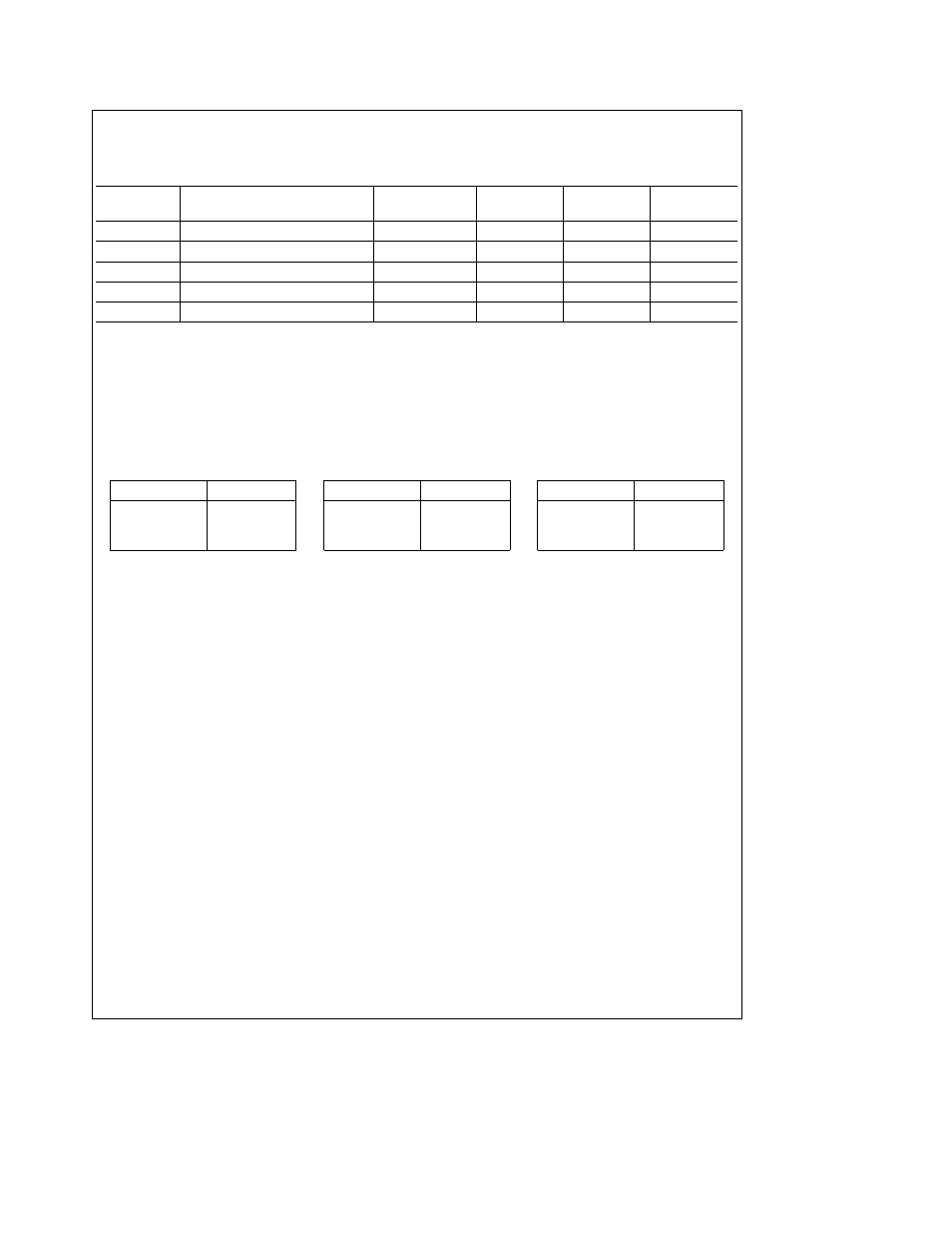
ADC10061
Suffix
i
JA
( C W)
CMJ
54
BIN CIN
70
BIWM CIWM
85
ADC10062
Suffix
i
JA
( C W)
CMJ
48
BIN CIN
60
BIWM CIWM
82
ADC10064
Suffix
i
JA
( C W)
CMJ
44
BIN CIN
53
BIWM CIWM
78
Note 5
Human body model 100 pF discharged through a 1 5 kX resistor
Note 6
See AN-450 ‘‘Surface Mounting Methods and Their Effect on Product Reliability’’ or the section titled ‘‘Surface Mount’’ found in a current National
Semiconductor Linear Data Book for other methods of soldering surface mount devices
Note 7
Typicals are at
a
25 C and represent must likely parametric norm
Note 8
Limits are guaranteed to National’s AOQL (Average Outgoing Quality Level)
Note 9
Accuracy may degrade if t
SH
is shorter than the value specified See curves of Accuracy vs t
SH
Note 10
A military RETS electrical test specification is available on request At time of printing the ADC10061CMJ 883 ADC10062CMJ 883 and
ADC10064CMJ 883 RETS specification complies fully with the boldface limits in this column
4