Functional description – Rainbow Electronics ADC10064 User Manual
Page 10

Functional Description
The ADC10061 ADC10062 and ADC10064 digitize an ana-
log input signal to 10 bits accuracy by performing two lower-
resolution ‘‘flash’’ conversions The first flash conversion
provides the six most significant bits (MSBs) of data and
the second flash conversion provides the four least signifi-
cant bits LSBs)
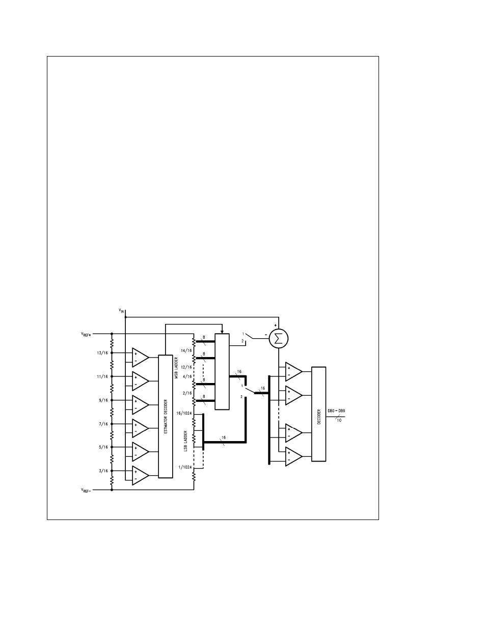
Figure 3
is a simplified block diagram of the converter Near
the center of the diagram is a string of resistors At the
bottom of the string of resistors are 16 resistors each of
which has a value 1 1024 the resistance of the whole resis-
tor string These lower 16 resistors (the LSB Ladder) there-
fore have a voltage drop of 16 1024 or 1 64 of the total
reference voltage (V
REF
a
b
V
REF
b
) across them The re-
mainder of the resistor string is made up of eight groups of
eight resistors connected in series These comprise the
MSB Ladder
Each section of the MSB Ladder has
of the
total reference voltage across it and each of the LSB resis-
tors has 1 64 of the total reference voltage across it Tap
points across these resistors can be connected in groups
of sixteen to the sixteen comparators at the right of the
diagram
On the left side of the diagram is a string of seven resistors
connected between V
REF
a
and V
REF
b
Six comparators
compare the input voltage with the tap voltages on this re-
sistor string to provide a low-resolution ‘‘estimate’’ of the
input voltage This estimate is then used to control the multi-
plexer that connects the MSB Ladder to the sixteen com-
parators on the right Note that the comparators on the left
needn’t be very accurate they simply provide an estimate of
the input voltage Only the sixteen comparators on the right
and the six on the left are necessary to perform the initial
six-bit flash conversion instead of the 64 comparators that
would be required using conventional half-flash methods
To perform a conversion the estimator compares the input
voltage with the tap voltages on the seven resistors on the
left The estimator decoder then determines which MSB
Ladder tap points will be connected to the sixteen compara-
tors on the right For example assume that the estimator
determines that V
IN
is between 11 16 and 13 16 of V
REF
The estimator decoder will instruct the comparator MUX to
connect the 16 comparators to the taps on the MSB ladder
between 10 16 and 14 16 of V
REF
The 16 comparators will
then perform the first flash conversion Note that since the
comparators are connected to ladder voltages that extend
beyond the range indicated by the estimator circuit errors in
the estimator as large as 1 16 of the reference voltage
(64 LSBs) will be corrected This first flash conversion pro-
duces the six most significant bits of data
four bits in the
flash itself and 2 bits in the estimator
The remaining four LSBs are now determined using the
same sixteen comparators that were used for the first flash
conversion The MSB Ladder tap voltage just below the in-
put voltage (as determined by the first flash) is subtracted
from the input voltage and compared with the tap points on
the sixteen LSB Ladder resistors The result of this second
four-bit flash conversion is then decoded and the full 10-bit
result is latched
Note that the sixteen comparators used in the first flash
conversion are reused for the second flash Thus the mul-
tistep conversion technique used in the ADC10061
ADC10062 and ADC10064 needs only a small fraction of
the number of comparators that would be required for a
traditional flash converter and far fewer than would be used
in a conventional half-flash approach
This allows the
ADC10061 ADC10062 and ADC10064 to perform high-
speed conversions without excessive power drain
TL H 11020 – 14
FIGURE 3 Block Diagram of the Multistep Converter Architecture
10
