Table 1. full-scale output current and r, Table 2. dac output code table – Rainbow Electronics MAX5550 User Manual
Page 9
I
2
C Compatibility (SPI/
I2C
= GND)
The MAX5550 is compatible with existing I
2
C systems
(
Figure 2). SCL and SDA are high-impedance inputs;
SDA has an open-drain output that pulls the data line
low during the ninth clock pulse. SDA and SCL require
pullup resistors (2.4k
Ω or greater) to V
DD
. Optional
resistors (24
Ω) in series with SDA and SCL protect the
device inputs from high-voltage spikes on the bus lines.
Series resistors also minimize crosstalk and undershoot
of the bus signals. The communication protocol sup-
ports standard I
2
C 8-bit communications. The device’s
address is compatible with 7-bit I
2
C addressing proto-
col only. Ten-bit address formats are not supported.
Only write commands are accepted by the MAX5550.
Note: I
2
C readback is not supported.
Bit Transfer
One data bit transfers during each SCL rising edge.
The MAX5550 requires nine clock cycles to transfer
data into or out of the DAC register. The data on SDA
must remain stable during the high period of the SCL
clock pulse. Changes in SDA while SCL is high are
read as control signals (see the START and STOP
Conditions section). Both SDA and SCL idle high.
START and STOP Conditions
The master initiates a transmission with a START condi-
tion (S), (a high-to-low transition on SDA with SCL high).
The master terminates a transmission with a STOP con-
dition (P), (a low-to-high transition on SDA while SCL is
high) (Figure 3). A START condition from the master
signals the beginning of a transmission to the
MAX5550. The master terminates transmission by issu-
ing a STOP condition. The STOP condition frees the
bus. If a repeated START condition (S
r
) is generated
instead of a STOP condition, the bus remains active.
MAX5550
Dual, 10-Bit, Programmable, 30mA
High-Output-Current DAC
_______________________________________________________________________________________
9
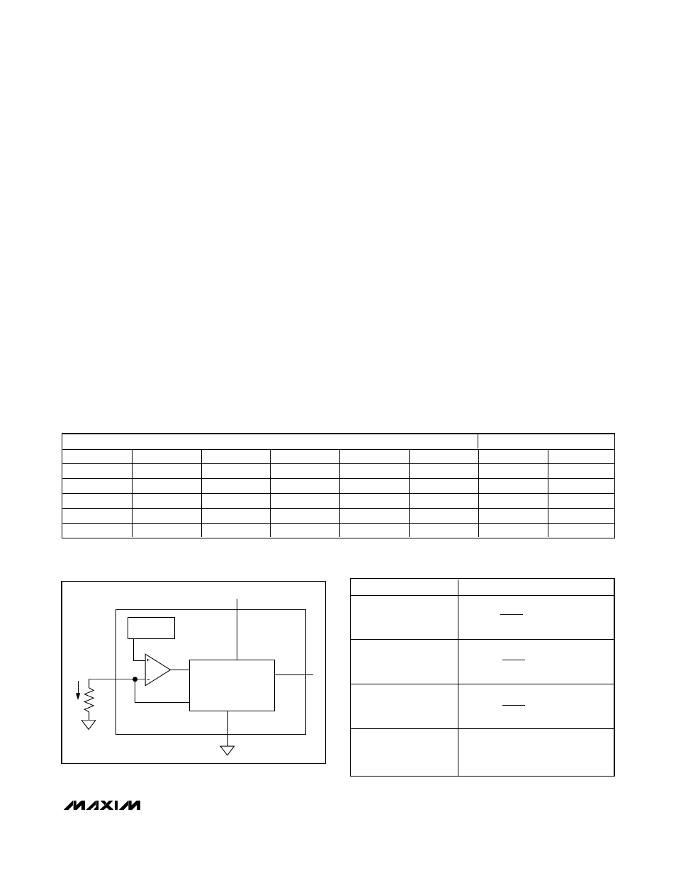
+1.25V
REFERENCE
I
FSADJ
R
FSADJ
FSADJ_
OUT_
V
DD
GND
CURRENT-SOURCE
ARRAY DAC
Figure 1. Reference Architecture and Output Current Adjustment
*Negative output current values = 0
FULL-SCALE OUTPUT CURRENT (mA)*
R
FSADJ
(k
Ω)
1mA–2mA
1.5mA–3mA
2.5mA–5mA
4.5mA–9mA
8mA–16mA
15mA–30mA
Calculated
1% EIA Std
1.00
1.500
2.500
4.500
8.00
15.00
40
40.2
1.25
1.875
3.125
5.625
10.00
18.75
35
34.8
1.50
2.250
3.750
6.750
12.00
22.50
30
30.1
1.75
2.625
4.375
7.875
14.00
26.25
25
24.9
2.00
3.000
5.000
9.000
16.00
30.00
20
20.0
Table 1. Full-Scale Output Current and R
FSADJ_
Selection Based on a +1.25V (typ)
Reference Voltage
*See the command summary in Table 4.
DAC CODE
I
OUT
_
11 1111 1111
10 0000 0000
00 0000 0001*
00 0000 0000
0
Table 2. DAC Output Code Table
1023
1024
×
−
I
I
I
FS
OS
|
|
1023
1024
×
−
I
I
FS
OS
|
|
1023
1024
×
−
I
I
FS
OS
|
|